Digilent D2-SB User Manual
Page 4
D2-SB Reference Manual
Digilent, Inc.
www.digilentinc.com
© Digilent, Inc.
Page 4
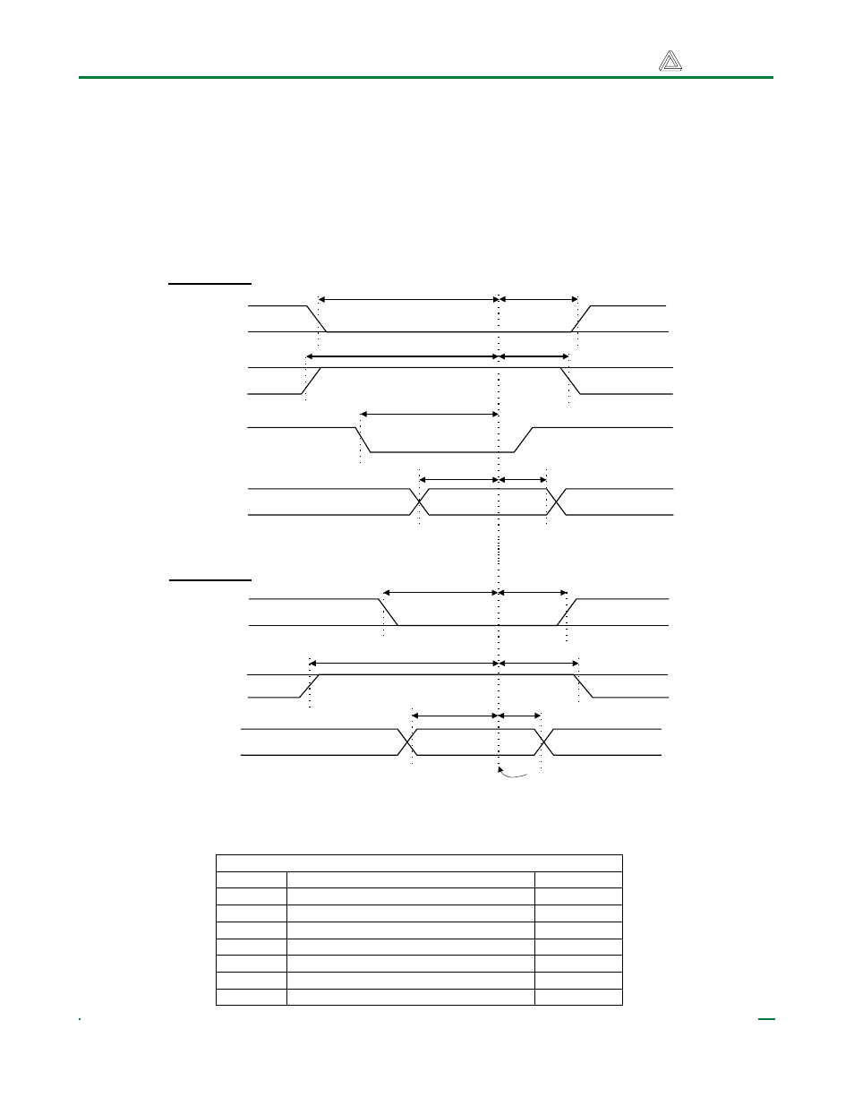
System Bus
The “system bus” is a protocol used by certain
expansion boards that mimics a simple 8-bit
microprocessor bus. It uses eight data lines,
six address lines, a write-enable (WE) strobe
that can be used by the peripheral to latch
written data, an output-enable (OE) strobe that
can be used by the peripheral to enable read
data, a chip select, and a clock to enable
synchronous transfers. The diagrams, (Figure
3), below show signal timings assumed by
Digilent to create peripheral devices. However,
any bus and timing models can be used by
modifying circuits in the FPGA and attached
peripheral devices.
tw
th
OE
CS
WE
DB0-DB7
th
teoe
tsu
tdoe
twd
th
OE
WE
DB0-DB7
teoe
tsu
tdoe
ten
Read data latch time
th
Write Cycle
Read Cycle
Figure 3. System Bus Timing
Table 1. System Bus Timing
Symbol
Parameter
Time (typ)
ten
Time to enable after CS asserted
10ns
th
Hold time
1ns
tdoe
Time to disable after OE de-asserted
10ns
teoe
Time to enable after OE asserted
15ns
tw
Write strobe time
10ns
tsu
Data setup time
5ns
twd
Write disable time
0ns