Digilent D2-SB User Manual
Page 2
D2-SB Reference Manual
Digilent, Inc.
www.digilentinc.com
© Digilent, Inc.
Page 2
standard functions can be obtained from
Digilent (see www.digilentinc.com).
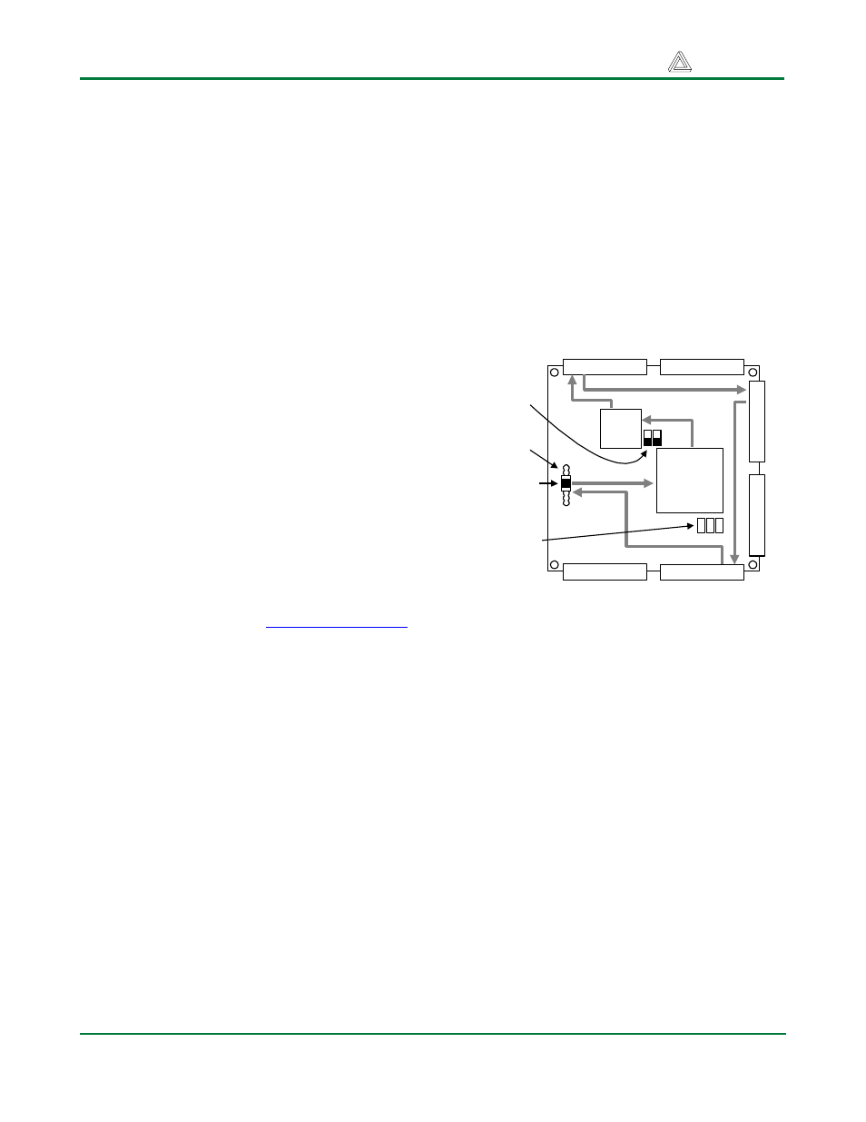
JTAG Ports and Device Configuration
The Spartan 2E FPGA , the 18V00 ROM on
the D2-SB, and any programmable devices on
peripheral boards attached to the D2-SB can
be programmed via the JTAG port. The JTAG
scan chain is routed to the FPGA and ROM on
the D2-SB and then around the board to four
connection ports as shown in Figure 2. The
primary configuration port (Port 1) uses a
standard 6-pin JTAG header (J7) that can
accommodate Digilent’s JTAG3 cable (or
cables from Xilinx or other vendors). The other
three JTAG programming ports are available
on the A1, B1, and C1 expansion connectors,
and these ports are bi-directional. If no
peripheral board is present, a buffer on the D2-
SB removes the expansion connector from the
JTAG chain. If a peripheral board with a JTAG
device is attached, the scan chain is driven out
the expansion connector so that any JTAG-
programmable parts can be configured. If a
Digilent port module is connected to one of the
three JTAG-enabled expansion connectors,
then the port module can drive the JTAG chain
to program all devices in the scan chain (port
modules include Ethernet, USB, EPP parallel,
and serial modules -- see
www.digilentinc.com
for more information).
The scan chain can be driven from the primary
port by powering on the D2-SB, connecting it
to a PC with a JTAG programming cable, and
running the “auto-detect” feature of the
configuration software. The configuration
software allows devices in the scan chain to be
selectively programmed with any available
configuration file. If no programming ROM is
loaded in the IC5 socket (or if ROM is present
but is not to be included in the scan chain),
jumper-shunts must be loaded at JP1 and JP2
in the “Bypass ROM” location to route the
JTAG chain around the ROM socket. If an
18V02 (or larger) ROM is loaded in the IC5
socket, it can be included in the scan chain by
loading the JP1 and JP2 jumper-shunts in the
“Include ROM” positions.
If a programming ROM is present in the IC5
socket, the FPGA will automatically access the
ROM for configuration data if jumper shunts
are loaded in all three positions of J8 (M2, M1,
and M0).
Port modules attached to ports A1, B1, or C1
can drive the scan chain if a jumper-shunt is
installed on the primary JTAG header across
the TDI and TDO pins. In their default state,
Digilent port modules will appear as a JTAG
cable to the configuration software. Port
modules can disable their JTAG drivers; if
more than one JTAG driver is enabled on the
scan chain, programming may fail.
A1
C2
Spartan 2E
PQ 208
A2
B1
B2
18V
ROM
JTAG
connector
Cable bypass
jumper
ROM bypass
jumpers
Programming
mode select
jumpers
C1
Port 1
Port 2
Port 3
Port 4
Figure 2. JTAG Signal Routing on D2-SB
Power Supplies
The D2-SB board uses two LM317 voltage
regulators to produce a 1.8VDC supply for the
Spartan 2E core, and 3.3VDC supply for the
I/O ring. Both regulators have good bypass
capacitance, allowing them to supply up to
1.5A of current with less than 50mV of noise
(typical). Power can be supplied from a low-
cost wall transformer supply. The external
supply must use a 2.1mm center-positive
connector, and it must produce between 6VDC
and 12VDC of unregulated voltage.
The D2-SB uses a four layer PCB, with the
inner layers dedicated to VCC and GND
planes. Most of the VCC plane is at 3.3V, with
an island under the FPGA at 1.8V. The FPGA
and the other ICs on the board all have
0.047uF bypass capacitors placed as close as
possible to each VCC pin.