Ac operating characteristics, Supported target devices – Digilent 410-205P-KIT User Manual
Page 4
JTAG-HS1™ Programming Cable for Xilinx® FPGAs
Copyright Digilent, Inc. All rights reserved.
Other product and company names mentioned may be trademarks of their respective owners.
Page 4 of 4
AC Operating Characteristics
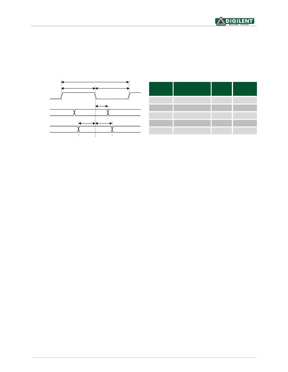
HS1 JTAG/SPI signals are driven according to the timing diagram below in Fig. 4. TCK frequencies from 30 MHz to 8
KHz are supported at integer divisions of 30 MHz from 1 to 3750. Common frequencies include 30 MHz, 15 MHz,
10 MHz, and 6 MHz (see Table 1).
Design Notes
The HS1 is designed to drive JTAG/SPI signals on target boards that have less than 100ohms of series resistance.
Higher resistance may result in degraded operation.
Supported Target Devices
The JTAG-HS1 is capable of targeting the following Xilinx devices:
1. Ordered List Item Xilinx FPGAs
2. Xilinx Zynq-7000
3. Xilinx CoolRunner™/CoolRunner-II CPLDs
4. Xilinx Platform Flash ISP configuration PROMs
5. Select third-party SPI PROMs
6. Select third-party BPI PROMs
The following devices cannot be targeted by the JTAG-HS1:
1. Ordered List ItemXilinx 9500/9500XL CPLDs
2. Xilinx 1700 and 18V00 ISP configuration PROMs
3. Xilinx FPGA eFUSE programming
Remote device configuration is not supported for the JTAG-HS1 when used with Xilinx's iMPACT software. Note:
Please see the "Introduction to Indirect Programming – SPI or BPI Flash Memory" help topic in iMPACT for a list of
supported FPGA/PROM combinations. Note: Please see the "Configuration Memory Support" section of Xilinx
UG908 for a list of the FPGA/PROM combinations that Vivado supports.
Symbol
Parameter
Min
Max
T
CK
T
CK
period
33ns
2.185ms
T
CKH
, T
CKL
T
CLK
pulse width
20ns
1.1ms
T
CD
T
CLK
to TMS, TDI
0
15ns
T
SU
TDO Setup time
19ns
T
HD
TDO Hold time
0
TMS/TDI
TCK
TDO
T
CKL
T
CKH
T
CK
T
CD
T
SU
T
HD
Figure 4. Timing diagram.
Table 1.Common frequencies.