Digilent 410-113P User Manual
Page 2

Document Title
Digilent Confidential
Digilent, Inc.
www.digilentinc.com Copyright Digilent, Inc.
Page
2
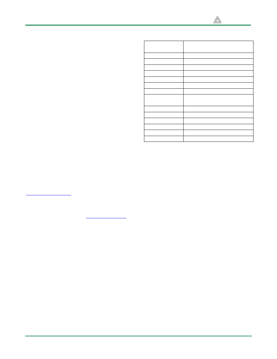
See Table 1 for a description of the signals on
the interface connectors J1 and J2. For
additional information, refer to the PmodDA2
schematic available on the Digilent web site at
www.digilentinc.com.
The PmodDA2 is usually powered from the
Digilent system board connected to it. The
power and ground connections are on pins five
and six of the digital interface connector J1.
Alternatively, the PmodDA2 can be powered
from an external power supply provided
through pins five and six of the analog
interface connector J2. In this case the power
select jumper on the system board should be
set to disconnect power from the system board
to J1. Damage may result if two power
supplies are connected at the same time.
The Digilent convention is to provide 3.3V to
power Pmod modules. The PmodDA2 can be
operated at any power supply voltage between
2.7V and 5.5V, however caution should be
exercised if using any voltage greater than
3.3V, as damage to the Digilent system board
could result. For more information refer to
reference manuals or schematics for the
system board available at
www.digilentinc.com
.
For detailed information about the National
Semiconductor data sheet refer to the National
Semiconductor web site at
www.national.com
.
Table 1: Interface Connector Signal
Descriptions
Digital
Interface – J1
1 SYNC
(common)
2
DINA (converter IC1)
3
DINB (converter IC2)
4 SCLK
(common)
5 GND
6 VCC
Analog
Interface – J2
1
VOUTA (converter IC1)
2 N/C
3
VOUTB (converter IC2)
4 N/C
5 GND
6 VCC
