Digilent 410-302P-KIT User Manual
Page 5
WiFire Reference Manual
The input voltage to the 5V regulator is taken from the VU bus, and the output is placed on the VCC5V0 power bus.
There is a reverse polarity protection diode in the external power supply circuit. Considering the diode drop plus
the forward drop across the regulator, the minimum input voltage to the regulator should be 7V to produce a
reliable 5V output.
For input voltages above 9V, the regulator will get extremely hot when drawing high currents. The NCP1117LP has
output short circuit protection as well as internal thermal protection and will shut down automatically to prevent
damage.
The 5V regulator selection on JP17 provides four 5V power configurations:
1) 5V regulator completely disabled and no 5V power available;
2) 5V regulator bypassed and 5V provided from an external 5V power supply, such as USB;
3) on-board 5V regulator used to provide 5V power;
4) External 5V regulator used to regulate VU and provide 5V power.
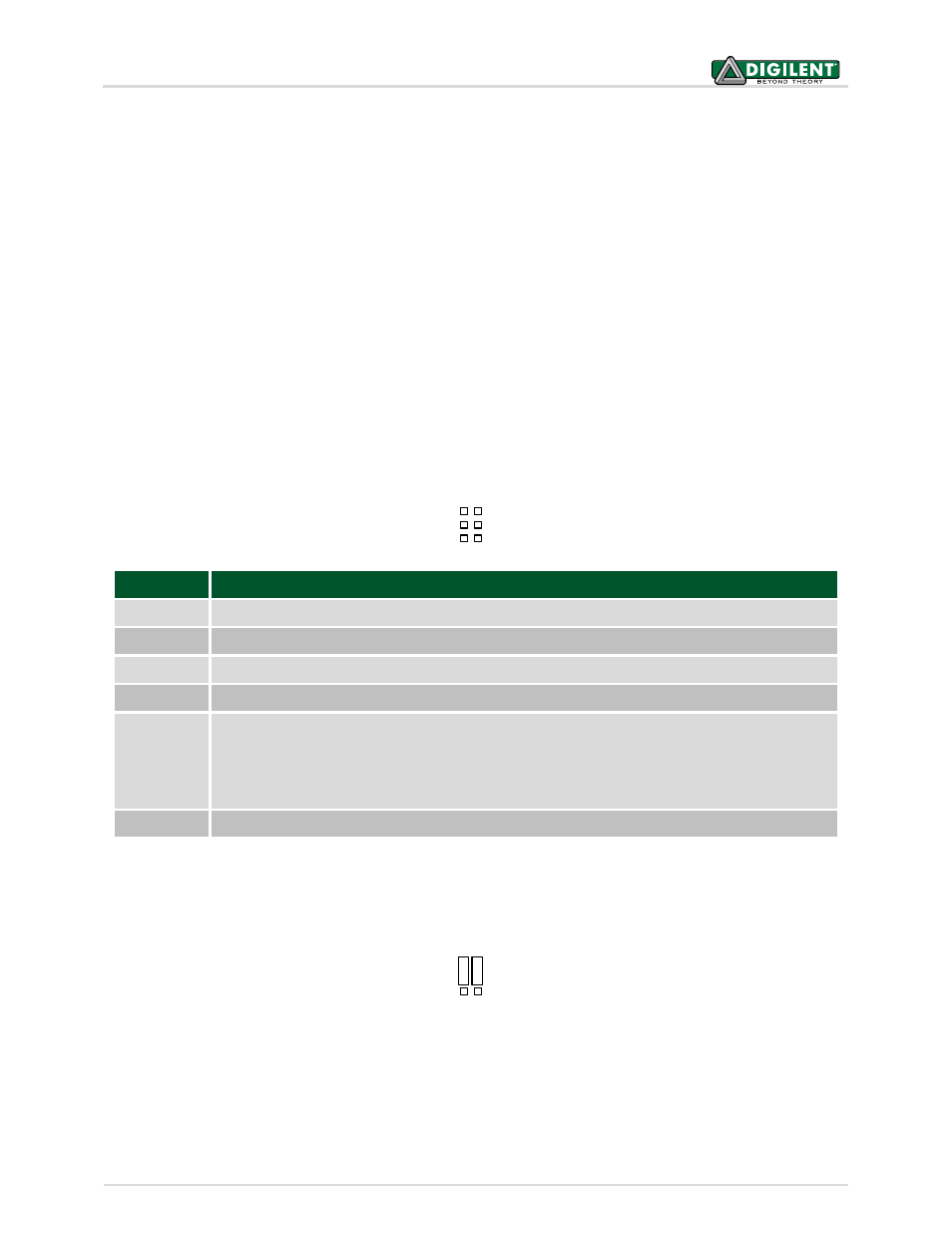
Jumper block J17 is used to select these various options and the following diagrams describe the use of J16. This
diagram shows the arrangement of the signals on J17:
LDO Out
LDO In
VU
5V0
GND
EN Ext
Signals
Description
LDO In
The input to the on-board linear regulator.
LDO Out
The output of the on-board regulator.
VU
The unregulated input voltage selected by the jumper setting jumper block J16.
5V0
The connection to the VCC5V0 power bus on the WiFire board.
EN Ext
Signal provided to enable an external voltage regulator, if one is being used. This would allow
the sketch running on the WiFire to turn on/off the external voltage regulator. When used with
an external voltage regulator, this allows the board to go into an extremely low power operating
mode. This signal is connected to Port D, bit 13 (RD13) on the PIC32 microcontroller. This is
accessible using digital pin 50.
GND
Connection to the digital ground bus on the WiFire board.
Table 2. Description of signals on J17.
To completely disable operation of the on-board linear regulator, remove all shorting blocks from J17. To use the
on-board 5V regulator, use the provided shorting blocks to connect VU to LDO In, and to connect LDO Out to 5V0,
as follows:
LDO Out
LDO In
VU
5V0
GND
EN Ext
Note: In this case, when J16 is in the EXT position, and J17 is jumpered to regulate the external input, do not apply
more than 18V; this can destroy the 5.0V regulator.
To bypass the on-board 5V regulator when powering the board from an externally regulator 5V power supply, such
as USB, Use one of the provided shorting blocks to connect VU to 5V0, as follows:
Copyright Digilent, Inc. All rights reserved.
Other product and company names mentioned may be trademarks of their respective owners.
Page 5 of 23