Capacitance, Thermal resistance, Ac test loads and waveforms – Cypress CY7C1018DV33 User Manual
Page 3
CY7C1018DV33
Document #: 38-05465 Rev. *D
Page 3 of 9
Capacitance
[3]
Parameter
Description
Test Conditions
Max.
Unit
C
IN
Input Capacitance
T
A
= 25°C, f = 1 MHz, V
CC
= 3.3V
8
pF
C
OUT
Output Capacitance
8
pF
Thermal Resistance
[3]
Parameter
Description
Test Conditions
400-Mil
Wide SOJ
Unit
Θ
JA
Thermal Resistance
(Junction to Ambient)
Still Air, soldered on a 3 × 4.5 inch,
four-layer printed circuit board
57.61
°C/W
Θ
JC
Thermal Resistance
(Junction to Case)
40.53
°C/W
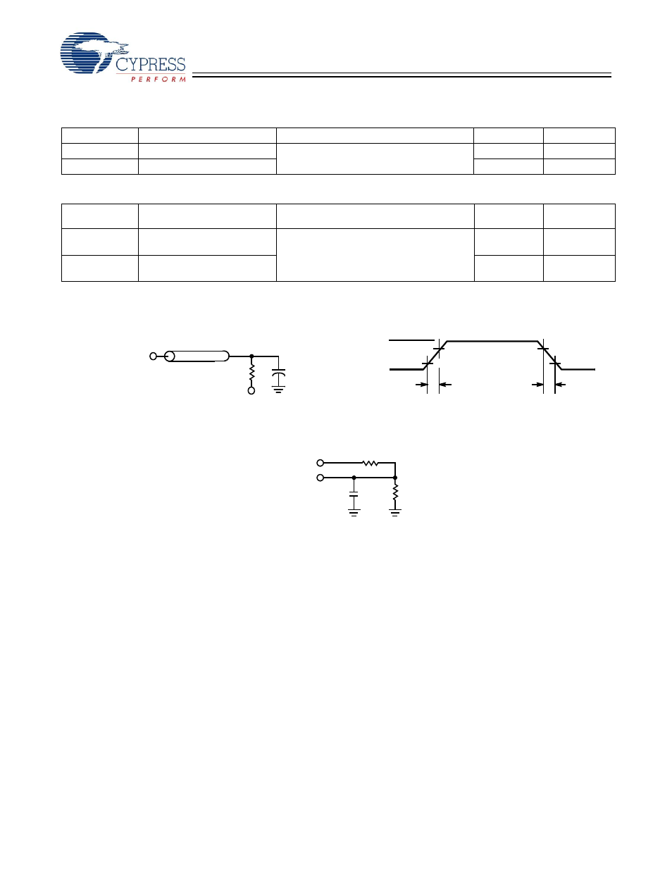
AC Test Loads and Waveforms
[4]
90%
10%
3.0V
GND
90%
10%
ALL INPUT PULSES
* CAPACITIVE LOAD CONSISTS
OF ALL COMPONENTS OF THE
TEST ENVIRONMENT
Rise Time: 1 V/ns
Fall Time: 1 V/ns
30 pF*
OUTPUT
Z = 50
Ω
50
Ω
1.5V
(b)
(a)
3.3V
OUTPUT
5 pF
(c)
R 317
Ω
R2
351
Ω
High-Z characteristics:
Notes
3. Tested initially and after any design or process changes that may affect these parameters.
4. AC characteristics (except High-Z) are tested using the load conditions shown in Figure (a). High-Z characteristics are tested for all speeds using the test load
shown in Figure (c).