Maximum ratings, Operating range, Electrical characteristics – Cypress CY62148E User Manual
Page 3: Capacitance
CY62148E MoBL
®
Document #: 38-05442 Rev. *F
Page 3 of 10
Maximum Ratings
Exceeding maximum ratings may impair the useful life of the
device. These user guidelines are not tested.
Storage Temperature ................................ –65°C to + 150°C
Ambient Temperature with
Power Applied............................................ –55°C to + 125°C
Supply Voltage to Ground
Potential.................................–0.5V to 6.0V (V
CCmax
+ 0.5V)
DC Voltage Applied to Outputs
in High-Z State
................–0.5V to 6.0V (V
CCmax
+ 0.5V)
DC Input Voltage
............ –0.5V to 6.0V (V
CCmax
+ 0.5V)
Output Current into Outputs (LOW)............................. 20 mA
Static Discharge Voltage........................................... > 2001V
(per MIL-STD-883, Method 3015)
Latch-up Current ......................................................>200mA
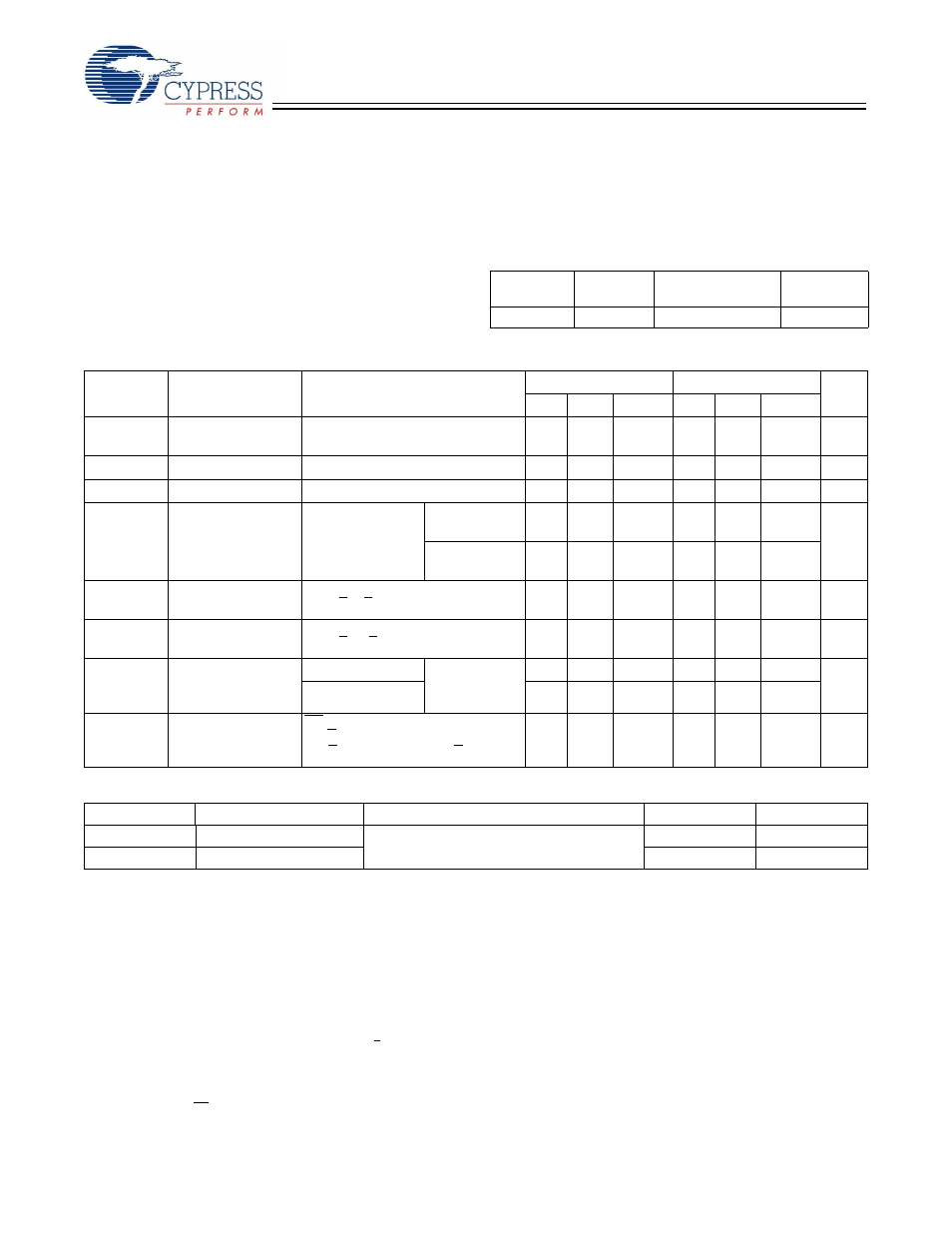
Operating Range
Device
Range
Ambient
Temperature
V
CC
CY62148E
Ind’l/Auto-A
–40°C to +85°C
4.5V to 5.5V
Electrical Characteristics
(Over the Operating Range)
Parameter
Description
Test Conditions
45 ns
55 ns
Unit
Min Typ
[3]
Max
Min Typ
Max
V
OH
Output HIGH
Voltage
I
OH
= –1 mA
2.4
2.4
V
V
OL
Output LOW Voltage I
OL
= 2.1 mA
0.4
0.4
V
V
IH
Input HIGH Voltage V
CC
= 4.5V to 5.5V
2.2
V
CC
+ 0.5 2.2
V
CC
+ 0.5
V
V
IL
Input LOW voltage
V
CC
= 4.5V to 5.5V For TSOPII
package
–0.5
0.8
V
For SOIC
package
–0.5
0.6
[8]
I
IX
Input Leakage
Current
GND < V
I
< V
CC
–1
+1
–1
+1
µA
I
OZ
Output Leakage
Current
GND < V
O
< V
CC
, Output Disabled
–1
+1
–1
+1
µA
I
CC
V
CC
Operating
Supply Current
f = f
max
= 1/t
RC
V
CC
= V
CC(max)
I
OUT
= 0 mA
CMOS levels
15
20
15
20
mA
f = 1 MHz
2
2.5
2
2.5
I
SB2
Automatic CE Power
down Current —
CMOS Inputs
CE > V
CC
– 0.2V
V
IN
> V
CC
– 0.2V or V
IN
< 0.2V,
f = 0, V
CC
= V
CC(max)
1
7
1
7
µA
Capacitance
(For All Packages)
Parameter
Description
Test Conditions
Max
Unit
C
IN
Input Capacitance
T
A
= 25°C, f = 1 MHz,
V
CC
= V
CC(typ)
10
pF
C
OUT
Output Capacitance
10
pF
Notes
5. V
IL(min)
= –2.0V for pulse durations less than 20 ns for I < 30 mA.
6. V
IH(max)
= V
CC
+0.75V for pulse durations less than 20 ns.
7. Full device AC operation assumes a minimum of 100 µs ramp time from 0 to V
CC
(min) and 200 µs wait time after V
CC
stabilization.
8. Under DC conditions the device meets a V
IL
of 0.8V. However, in dynamic conditions Input LOW Voltage applied to the device must not be higher than 0.6V. This
is applicable to SOIC package only. Refer to AN13470 for details.
9. Only chip enable (CE) must be HIGH at CMOS level to meet the I
SB2
spec. Other inputs can be left floating.
10. Tested initially and after any design or process changes that may affect these parameters.