Cy2048waf, Absolute maximum conditions, Crystal specifications – Cypress CY2048WAF User Manual
Page 3: Operating conditions, Dc electrical specifications

CY2048WAF
Document #: 38-07738 Rev. *A
Page 3 of 7
Absolute Maximum Conditions
(Above which the useful life may be impaired.
For user guidelines, not tested.)
Supply Voltage (V
DD
) ........................................–0.5 to +7.0V
DC Input Voltage ...................................... –0.5V to V
DD
+ 0.5
Output Short Circuit Current ..................................... ± 50 mA
Storage Temperature (Non-condensing) .... –55°C to +125°C
Junction Temperature ................................ –40°C to +125°C
Data Retention @ Tj = 125°C................................> 10 years
ESD (Human Body Model) MIL-STD-883................. > 2000V
Note:
1. Not 100% tested.
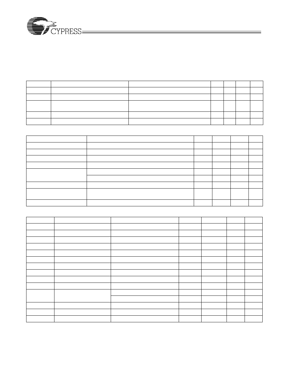
Crystal Specifications
[1]
Parameter
Description
Comments
Min.
Typ.
Max.
Unit
F
NOM
Nominal crystal frequency
Fundamental mode, AT cut
10
–
48
MHz
R
1
Equivalent series resistance (ESR)
Fundamental mode
–
–
40
Ω
R
3
/R
1
Ratio of third overtone mode ESR to
fundamental mode ESR
Ratio used because typical R
1
values are
much less than the maximum spec
4.5
–
–
–
C
0
Crystal shunt capacitance
–
–
5
pF
C
1
Crystal motional capacitance
2
–
–
fF
Operating Conditions
Parameter
Description
Min.
Typ.
Max.
Unit
V
DD
Operating Voltage
2.7
–
3.6
V
T
J
Junction Temperature
–40
–
125
°C
C
XIN
Capacitance XIN, all tuning caps OFF
–
10
–
pF
C
XOUT
Capacitance XOUT, all tuning caps OFF
–
10
–
pF
C
L
All tuning Caps OFF
4
5
6
pF
All tuning Caps ON
9.2
10
11.4
pF
C
OUT
Output Load Capacitance
–
–
15
pF
t
RAMP
Power-up time for V
DD
to reach minimum specified
voltage (power ramps must be monotonic)
0.05
–
500
ms
T
S
Start up time, 90% V
DD
to valid frequency on output
–
–
10
ms
DC Electrical Specifications
TJ = –40 to 125°C over the operating range
Parameter
Description
Condition
Min.
Typ.
Max.
Unit
V
IL
Input Low Voltage
CMOS Levels
–
–
20
%VDD
V
IH
Input High Voltage
CMOS Levels
80
–
–
%VDD
V
OL
Output Low Voltage
V
DD
= 2.7V–3.6V, I
OL
= 8 mA
–
–
0.4
V
V
OH
Output High Voltage
V
DD
= 2.7V–3.6V, I
OL
= –8 mA
V
DD
–0.4
–
–
V
I
IL
Input Low Current
Input = V
SS
–
1
10
µA
I
IH
Input High Current
Input = V
DD
–
1
10
µA
I
OZL
Output Leakage Current
Output = V
SS
–
1
10
µA
I
OZH
Output Leakage Current
Output = V
DD
–
–
50
µA
I
DD
Power Supply Current
No Load, V
DD
= 3.3V, 48 MHz
–
–
20
mA
I
PD
Power Down Current
PD# = 0V
–
–
25
µA
R
UP
Input Pull-up resistor
V
IN
= V
SS
1
3
6
M
Ω
V
IN
> = 0.8V
DD
80
120
150
k
Ω
R
DN
Output Pull-down resistor
V
IN
= 0.5V
DD
500
900
1500
k
Ω
C
IN
Input Pin Capacitance
PD#/OE pin
–
–
7
pF
R
F
Crystal Feedback R
XIN = 0
300
–
800
k
Ω
