Cypress CY2048WAF User Manual
Cy2048waf, Features, Benefits

Flash Programmable Capacitor Tuning Array Die
for Crystal Oscillator(XO)
CY2048WAF
Cypress Semiconductor Corporation
•
3901 North First Street
•
San Jose
,
CA 95134
•
408-943-2600
Document #: 38-07738 Rev. *A
Revised December 12, 2005
Features
• Flash-programmable capacitor tuning array for low
ppm initial frequency clock output
• Low clock output jitter
— 4 ps typ. RMS period jitter
— ±30 ps typ. peak-to-peak period jitter
• Flash-programmable dividers
• Two-pin programming interface
• On-chip oscillator runs from 10–48-MHz crystal
• Five selectable post-divide options, using reference
oscillator output
• Programmable asynchronous or synchronous OE and
PWR_DWN modes
• 2.7V to 3.6V operation
• Controlled rise and fall times and output slew rate
Benefits
• Enables fine-tuning of output clock frequency by
adjusting C
Load
of the crystal
• Allows multiple programming opportunities to correct
errors, and control excess inventory
• Enables programming of output frequency after
packaging
• PPM clock output error can be adjusted in package
• Provides flexibility in output configurations and testing
• Enables low-power operation or output enable function
• Provides flexibility for system applications through
selectable instantaneous or synchronous change in
outputs
• Enables encapsulation in small-size, surface-mount
packages
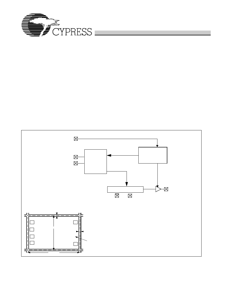
Block Diagram
Die Pad Description
H o riz o n ta l S c rib e
V e rtic a l
S c rib e
Y (m a x )
X (m a x )
6
O U T
2
3
4
V D D
X IN
P D # /O E
5
7 C 8 0 3 3 0 A
1
X O U T
d ie # /r e v
V S S
Notes
:
X(max): 980
µm, Y(max): 988 µm
Bond pad opening: 85
µm x 85 µm
Pad pitch: 175
µm (min.)
Scribe: X = 70
µm, Y = 86 µm
Wafer thickness: 11 mils (Typ.)
PD#/OE
VSS
VDD
(SDATA/VPP)
XIN
XOUT
CRYSTAL
OUT
/ 1, 2, 4, 8, 16
OSCILLATOR
CONFIGURATION
(SCL)
