Pin definitions – Cypress CY7C1318CV18-200BZI User Manual
Page 5
CY7C1318CV18
CY7C1320CV18
Document Number: 001-07160 Rev. *F
Page 5 of 26
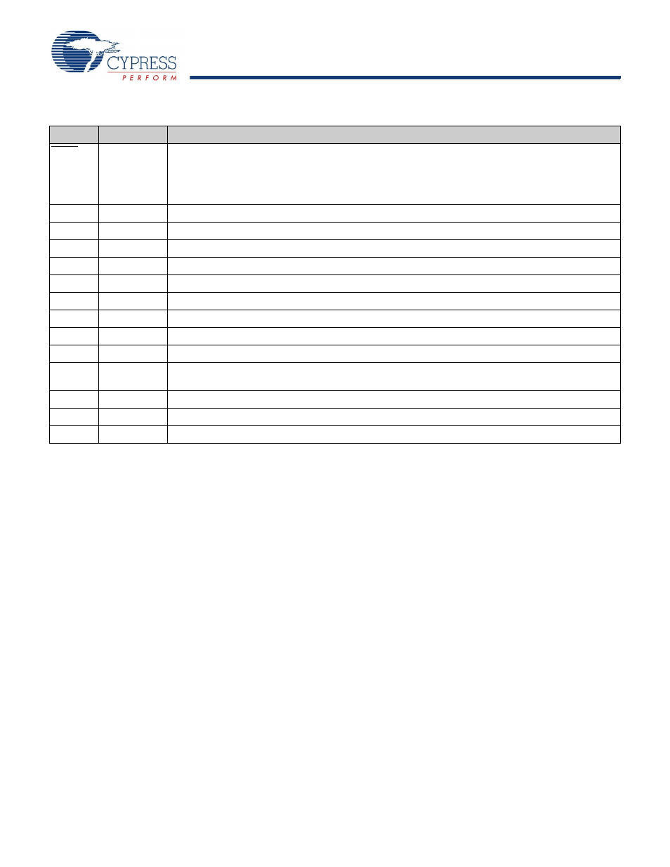
DOFF
Input
DLL Turn Off
− Active LOW. Connecting this pin to ground turns off the DLL inside the device. The timing
in the DLL turned off operation is different from that listed in this data sheet. For normal operation, this
pin can be connected to a pull up through a 10 K
Ω or less pull up resistor. The device behaves in DDR I
mode when the DLL is turned off. In this mode, the device can be operated at a frequency of up to 167
MHz with DDR I timing.
TDO
Output
TDO for JTAG.
TCK
Input
TCK Pin for JTAG.
TDI
Input
TDI Pin for JTAG.
TMS
Input
TMS Pin for JTAG.
NC
N/A
Not Connected to the Die. Can be tied to any voltage level.
NC/36M
N/A
Not Connected to the Die. Can be tied to any voltage level.
NC/72M
N/A
Not Connected to the Die. Can be tied to any voltage level.
NC/144M
N/A
Not Connected to the Die. Can be tied to any voltage level.
NC/288M
N/A
Not Connected to the Die. Can be tied to any voltage level.
V
REF
Input-
Reference
Reference Voltage Input. Static input used to set the reference level for HSTL inputs, outputs, and AC
measurement points.
V
DD
Power Supply Power Supply Inputs to the Core of the Device.
V
SS
Ground
Ground for the Device.
V
DDQ
Power Supply Power Supply Inputs for the Outputs of the Device.
Pin Definitions
(continued)
Pin Name
I/O
Pin Description