Pin definitions – Cypress CY7C1318CV18-200BZI User Manual
Page 4

CY7C1318CV18
CY7C1320CV18
Document Number: 001-07160 Rev. *F
Page 4 of 26
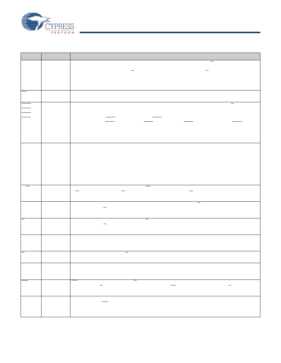
Pin Definitions
Pin Name
I/O
Pin Description
DQ
[x:0]
Input Output-
Synchronous
Data Input Output Signals. Inputs are sampled on the rising edge of K and K clocks during valid write
operations. These pins drive out the requested data during a read operation. Valid data is driven out on
the rising edge of both the C and C clocks during read operations or K and K when in single clock mode.
When read access is deselected, Q
[x:0]
are automatically tristated.
CY7C1318CV18
− DQ
[17:0]
CY7C1320CV18
− DQ
[35:0]
LD
Input-
Synchronous
Synchronous Load. This input is brought LOW when a bus cycle sequence is defined. This definition
includes address and read/write direction. All transactions operate on a burst of 2 data.
BWS
0
,
BWS
1
,
BWS
2
,
BWS
3
Input-
Synchronous
Byte Write Select 0, 1, 2, and 3
− Active LOW. Sampled on the rising edge of the K and K clocks during
write operations. Used to select which byte is written into the device during the current portion of the Write
operations. Bytes not written remain unaltered.
CY7C1318CV18
− BWS
0
controls D
[8:0]
and BWS
1
controls D
[17:9].
CY7C1320CV18
− BWS
0
controls D
[8:0]
, BWS
1
controls D
[17:9]
, BWS
2
controls D
[26:18]
and BWS
3
controls
D
[35:27]
.
All the Byte Write Selects are sampled on the same edge as the data. Deselecting a Byte Write Select
ignores the corresponding byte of data and it is not written into the device.
A, A0
Input-
Synchronous
Address Inputs. These address inputs are multiplexed for both read and write operations. Internally, the
device is organized as 1M x 18 (2 arrays each of 512K x 18) for CY7C1318CV18, and 512K x 36 (2 arrays
each of 256K x 36) for CY7C1320CV18.
CY7C1318CV18 – A0 is the input to the burst counter. These are incremented internally in a linear fashion.
20 address inputs are needed to access the entire memory array.
CY7C1320CV18 – A0 is the input to the burst counter. These are incremented internally in a linear fashion.
19 address inputs are needed to access the entire memory array. All the address inputs are ignored when
the appropriate port is deselected.
R/W
Input-
Synchronous
Synchronous Read/Write Input. When LD is LOW, this input designates the access type (read when
R/W is HIGH, write when R/W is LOW) for the loaded address. R/W must meet the setup and hold times
around the edge of K.
C
Input Clock
Positive Input Clock for Output Data. C is used in conjunction with C to clock out the read data from
the device. C and C can be used together to deskew the flight times of various devices on the board back
to the controller. See
on page 7 for more information.
C
Input Clock
Negative Input Clock for Output Data. C is used in conjunction with C to clock out the read data from
the device. C and C can be used together to deskew the flight times of various devices on the board back
to the controller. See
on page 7 for more information.
K
Input Clock
Positive Input Clock Input. The rising edge of K is used to capture synchronous inputs to the device
and to drive out data through Q
[x:0]
when in single clock mode. All accesses are initiated on the rising
edge of K.
K
Input Clock
Negative Input Clock Input. K is used to capture synchronous data being presented to the device and
to drive out data through Q
[x:0]
when in single clock mode.
CQ
Output Clock CQ Referenced with Respect to C. This is a free running clock and is synchronized to the input clock
for output data (C) of the DDR II. In single clock mode, CQ is generated with respect to K. The timing for
the echo clocks is shown in
CQ
Output Clock CQ Referenced with Respect to C. This is a free running clock and is synchronized to the input clock
for output data (C) of the DDR II. In single clock mode, CQ is generated with respect to K. The timing for
the echo clocks is shown in
ZQ
Input
Output Impedance Matching Input. This input is used to tune the device outputs to the system data bus
impedance. CQ, CQ, and Q
[x:0]
output impedance are set to 0.2 x RQ, where RQ is a resistor connected
between ZQ and ground. Alternatively, this pin can be connected directly to V
DDQ
, which enables the
minimum impedance mode. This pin cannot be connected directly to GND or left unconnected.
