Depth expansion, Programmable impedance, Echo clocks – Cypress Perform CY7C1413BV18 User Manual
Page 9: Application example

CY7C1411BV18, CY7C1426BV18
CY7C1413BV18, CY7C1415BV18
Document Number: 001-07037 Rev. *D
Page 9 of 30
includes forwarding data from a write cycle that was initiated on
the previous K clock rise.
Read accesses and write access must be scheduled such that
one transaction is initiated on any clock cycle. If both ports are
selected on the same K clock rise, the arbitration depends on the
previous state of the SRAM. If both ports were deselected, the
read port takes priority. If a read was initiated on the previous
cycle, the write port takes priority (as read operations can not be
initiated on consecutive cycles). If a write was initiated on the
previous cycle, the read port takes priority (as write operations
can not be initiated on consecutive cycles). Therefore, asserting
both port selects active from a deselected state results in alter-
nating read or write operations being initiated, with the first
access being a read.
Depth Expansion
The CY7C1413BV18 has a port select input for each port. This
enables for easy depth expansion. Both port selects are sampled
on the rising edge of the positive input clock only (K). Each port
select input can deselect the specified port. Deselecting a port
does not affect the other port. All pending transactions (read and
write) completes prior to the device being deselected.
Programmable Impedance
An external resistor, RQ, must be connected between the ZQ pin
on the SRAM and V
SS
to allow the SRAM to adjust its output
driver impedance. The value of RQ must be 5X the value of the
intended line impedance driven by the SRAM. The allowable
range of RQ to guarantee impedance matching with a tolerance
of ±15% is between 175
Ω and 350Ω
,
with V
DDQ
= 1.5V. The
output impedance is adjusted every 1024 cycles upon power up
to account for drifts in supply voltage and temperature.
Echo Clocks
Echo clocks are provided on the QDR-II to simplify data capture
on high-speed systems. Two echo clocks are generated by the
QDR-II. CQ is referenced with respect to C and CQ is referenced
with respect to C. These are free running clocks and are synchro-
nized to the output clock of the QDR-II. In the single clock mode,
CQ is generated with respect to K and CQ is generated with
respect to K. The timings for the echo clocks are shown in the
DLL
These chips use a Delay Lock Loop (DLL) that is designed to
function between 120 MHz and the specified maximum clock
frequency. During power up, when the DOFF is tied HIGH, the
DLL gets locked after 1024 cycles of stable clock. The DLL can
also be reset by slowing or stopping the input clock K and K for
a minimum of 30 ns. However, it is not necessary to reset the
DLL to lock to the desired frequency. The DLL automatically
locks 1024 clock cycles after a stable clock is presented. The
DLL may be disabled by applying ground to the DOFF pin. When
the DLL is turned off, the device behaves in QDR-I mode (with
one cycle latency and a longer access time). For information
refer to the application note “DLL Considerations in
QDRII/DDRII”.
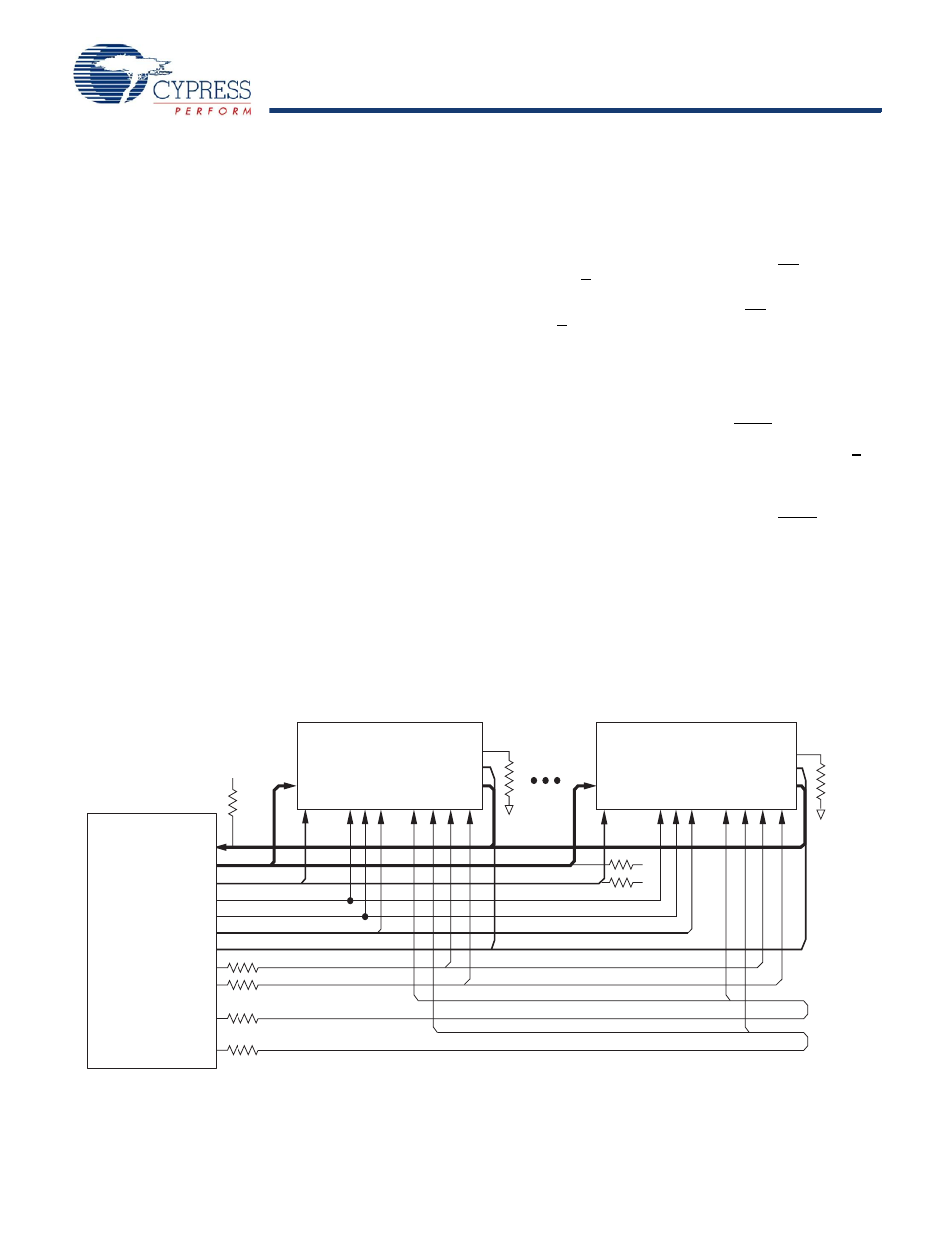
Application Example
shows four QDR-II used in an application.
Figure 1. Application Example
R = 250
ohms
Vt
R
R = 250
ohms
Vt
Vt
R
Vt = Vddq/2
R = 50
ohms
R
C C#
D
A
SRAM #4
R
P
S
#
W
P
S
#
B
W
S
#
K
ZQ
CQ/CQ#
Q
K#
C C#
D
A
K
SRAM #1
R
P
S
#
W
P
S
#
B
W
S
#
ZQ
CQ/CQ#
Q
K#
BUS
MASTER
(CPU
or
ASIC)
DATA IN
DATA OUT
Address
RPS#
WPS#
BWS#
Source K
Source K#
Delayed K
Delayed K#
CLKIN/CLKIN#
