1 i 2 i 3 i 4 i – Sony cdp 338esd User Manual
Page 7
Attention! The text in this document has been recognized automatically. To view the original document, you can use the "Original mode".
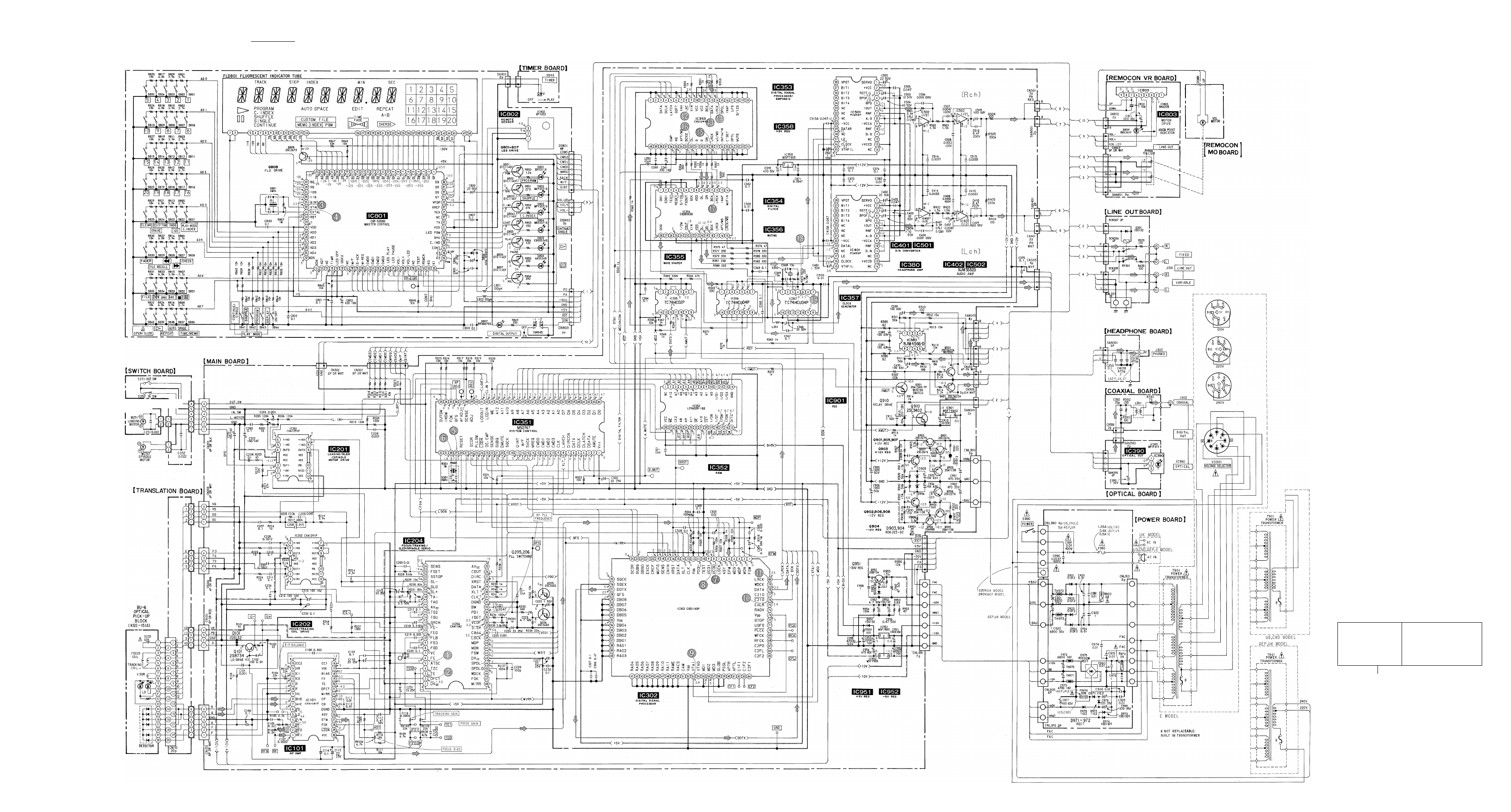
3-3. SCHEMATIC DIAGRAM • Refer to page 17 for Waveforms.
1 I 2 I 3 I 4 I
В
H
к
M
N
8
10
11
1 2
13
14
15
16
17
18
19
20
21
22
23
24
25
26
[DISPLAY BOARD]
[L.MOTOR BOARD]
Note on Schematic Diagram:
•
All
capacitors
are
in
juF
unless
otherwise
noted.
pF:
ju^tF
50WV
or
less
are
not
indicated
except
for
electrolytics
and tantalums.
•
All
resistors
are
in
SI
and
‘/
4
W
or
less
unless
otherwise
specified.
•
%
: indicates tolerance.
•
A
: internal component.
• "^^
3
": fusible resistor.
Note:
The components identi
fied by mark Дог dot
ted line with mark Д
are critical for safety.
Replace only with part
number specified.
Note:
Lés
composants
identifiés
par
une
marque^sont
critiques
pour la sécurité.
Ne
les
remplacer
que
par
une
pièce
portant
le
numéro
spéci
fié.
0 : 8+ L
ne
B- L
___ adjustment for repair.
Voltage and waveforms are dc with respect to ground
under no-signal conditions,
no mark : STOP
(
); PLAY
Voltages are taken with a VOM (Input impedance 1 OM Q )•
Voltage
variations
may
be
noted
due
to
normal
produc
tion tolerances.
Waveforms are taken with a oscilloscope.
Voltage
variations
may
be
noted
due
to
normal
produc
tion tolerances.
Circled numbers refer to waveforms.
Signal path.
^
: CD
13-
14
15-
-16