Truth table – Cypress CY7C1387FV25 User Manual
Page 9
CY7C1386DV25, CY7C1386FV25
CY7C1387DV25, CY7C1387FV25
Document Number: 38-05548 Rev. *E
Page 9 of 30
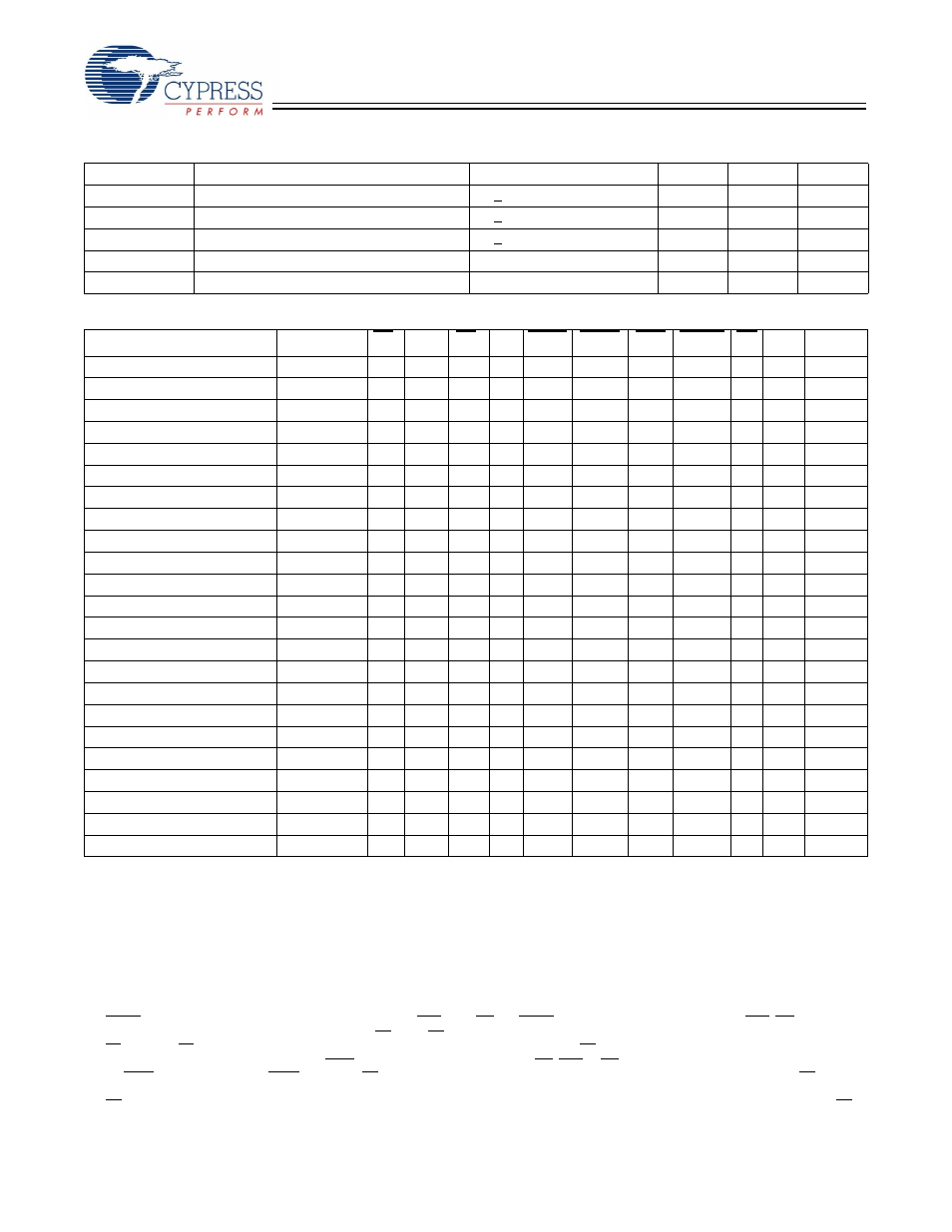
ZZ Mode Electrical Characteristics
Parameter
Description
Test Conditions
Min.
Max.
Unit
I
DDZZ
Sleep mode standby current
ZZ > V
DD
– 0.2V
80
mA
t
ZZS
Device operation to ZZ
ZZ > V
DD
– 0.2V
2t
CYC
ns
t
ZZREC
ZZ recovery time
ZZ < 0.2V
2t
CYC
ns
t
ZZI
ZZ Active to sleep current
This parameter is sampled
2t
CYC
ns
t
RZZI
ZZ Inactive to exit sleep current
This parameter is sampled
0
ns
Truth Table
Operation
Add. Used
CE
1
CE
2
CE
3
ZZ ADSP ADSC
ADV WRITE OE CLK
DQ
Deselect Cycle, Power Down
None
H
X
X
L
X
L
X
X
X
L-H Tri-State
Deselect Cycle, Power Down
None
L
L
X
L
L
X
X
X
X
L-H Tri-State
Deselect Cycle, Power Down
None
L
X
H
L
L
X
X
X
X
L-H Tri-State
Deselect Cycle, Power Down
None
L
L
X
L
H
L
X
X
X
L-H Tri-State
Deselect Cycle, Power Down
None
L
X
H
L
H
L
X
X
X
L-H Tri-State
Sleep Mode, Power Down
None
X
X
X
H
X
X
X
X
X
X
Tri-State
READ Cycle, Begin Burst
External
L
H
L
L
L
X
X
X
L
L-H
Q
READ Cycle, Begin Burst
External
L
H
L
L
L
X
X
X
H
L-H Tri-State
WRITE Cycle, Begin Burst
External
L
H
L
L
H
L
X
L
X
L-H
D
READ Cycle, Begin Burst
External
L
H
L
L
H
L
X
H
L
L-H
Q
READ Cycle, Begin Burst
External
L
H
L
L
H
L
X
H
H
L-H Tri-State
READ Cycle, Continue Burst
Next
X
X
X
L
H
H
L
H
L
L-H
Q
READ Cycle, Continue Burst
Next
X
X
X
L
H
H
L
H
H
L-H Tri-State
READ Cycle, Continue Burst
Next
H
X
X
L
X
H
L
H
L
L-H
Q
READ Cycle, Continue Burst
Next
H
X
X
L
X
H
L
H
H
L-H Tri-State
WRITE Cycle, Continue Burst
Next
X
X
X
L
H
H
L
L
X
L-H
D
WRITE Cycle, Continue Burst
Next
H
X
X
L
X
H
L
L
X
L-H
D
READ Cycle, Suspend Burst
Current
X
X
X
L
H
H
H
H
L
L-H
Q
READ Cycle, Suspend Burst
Current
X
X
X
L
H
H
H
H
H
L-H Tri-State
READ Cycle, Suspend Burst
Current
H
X
X
L
X
H
H
H
L
L-H
Q
READ Cycle, Suspend Burst
Current
H
X
X
L
X
H
H
H
H
L-H Tri-State
WRITE Cycle, Suspend Burst
Current
X
X
X
L
H
H
H
L
X
L-H
D
WRITE Cycle, Suspend Burst
Current
H
X
X
L
X
H
H
L
X
L-H
D
Notes
4. X = Don't Care, H = Logic HIGH, L = Logic LOW.
5. WRITE = L when any one or more byte write enable signals and BWE = L or GW = L. WRITE = H when all byte write enable signals, BWE, GW = H.
6. The DQ pins are controlled by the current cycle and the OE signal. OE is asynchronous and is not sampled with the clock.
7. CE
1
, CE
2
, and CE
3
are available only in the TQFP package. BGA package has only 2 chip selects CE
1
and CE
2
.
8. The SRAM always initiates a read cycle when ADSP is asserted, regardless of the state of GW, BWE, or BW
X
. Writes may occur only on subsequent clocks after
the ADSP or with the assertion of ADSC. As a result, OE must be driven HIGH prior to the start of the write cycle to allow the outputs to tri-state. OE is a don't
care for the remainder of the write cycle.
9. OE is asynchronous and is not sampled with the clock rise. It is masked internally during write cycles. During a read cycle all data bits are tri-state when OE is
inactive or when the device is deselected, and all data bits behave as output when OE is active (LOW).