Pin definitions – Cypress CY7C1334H User Manual
Page 3
CY7C1334H
Document #: 38-05678 Rev. *B
Page 3 of 13
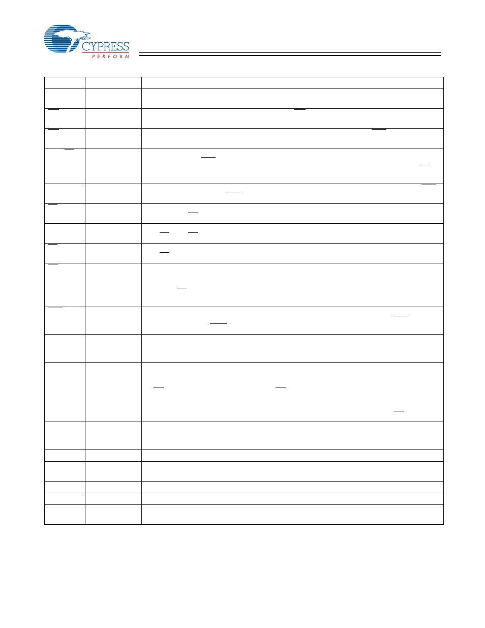
Pin Definitions
Name
I/O
Description
A0, A1, A
Input-
Synchronous
Address Inputs used to select one of the 64K address locations. Sampled at the rising edge
of the CLK. A
[1:0]
are fed to the two-bit burst counter.
BW
[A:D]
Input-
Synchronous
Byte Write Inputs, active LOW. Qualified with WE to conduct writes to the SRAM. Sampled
on the rising edge of CLK.
WE
Input-
Synchronous
Write Enable Input, active LOW. Sampled on the rising edge of CLK if CEN is active LOW.
This signal must be asserted LOW to initiate a Write sequence.
ADV/LD
Input-
Synchronous
Advance/Load Input. Used to advance the on-chip address counter or load a new address.
When HIGH (and CEN is asserted LOW) the internal burst counter is advanced. When LOW, a
new address can be loaded into the device for an access. After being deselected, ADV/LD
should be driven LOW in order to load a new address.
CLK
Input-Clock
Clock Input. Used to capture all synchronous inputs to the device. CLK is qualified with CEN.
CLK is only recognized if CEN is active LOW.
CE
1
Input-
Synchronous
Chip Enable 1 Input, active LOW. Sampled on the rising edge of CLK. Used in conjunction
with CE
2
and CE
3
to select/deselect the device.
CE
2
Input-
Synchronous
Chip Enable 2 Input, active HIGH. Sampled on the rising edge of CLK. Used in conjunction
with CE
1
and CE
3
to select/deselect the device.
CE
3
Input-
Synchronous
Chip Enable 3 Input, active LOW. Sampled on the rising edge of CLK. Used in conjunction
with CE
1
and
CE
2
to select/deselect the device.
OE
Input-
Asynchronous
Output Enable, asynchronous input, active LOW. Combined with the synchronous logic
block inside the device to control the direction of the I/O pins. When LOW, the I/O pins are
allowed to behave as outputs. When deasserted HIGH, I/O pins are tri-stated, and act as input
data pins. OE is masked during the data portion of a write sequence, during the first clock when
emerging from a deselected state, when the device has been deselected.
CEN
Input-
Synchronous
Clock Enable Input, active LOW. When asserted LOW the Clock signal is recognized by the
SRAM. When deasserted HIGH the Clock signal is masked. Since deasserting CEN does not
deselect the device, CEN can be used to extend the previous cycle when required.
ZZ
Input-
Asynchronous
ZZ “sleep” Input. This active HIGH input places the device in a non-time critical “sleep”
condition with data integrity preserved. During normal operation, this pin can be connected to
V
SS
or left floating.
DQs
I/O-
Synchronous
Bidirectional Data I/O Lines. As inputs, they feed into an on-chip data register that is triggered
by the rising edge of CLK. As outputs, they deliver the data contained in the memory location
specified by A
[16:0]
during the clock rise of the read cycle. The direction of the pins is controlled
by OE and the internal control logic. When OE is asserted LOW, the pins can behave as outputs.
When HIGH, DQ
s
are placed in a tri-state condition. The outputs are automatically tri-stated
during the data portion of a write sequence, during the first clock when emerging from a
deselected state, and when the device is deselected, regardless of the state of OE.
MODE
Input
Strap pin
Mode Input. Selects the burst order of the device.
When tied to Gnd selects linear burst sequence. When tied to V
DD
or left floating selects inter-
leaved burst sequence.
V
DD
Power Supply
Power supply inputs to the core of the device.
V
DDQ
I/O Power
Supply
Power supply for the I/O circuitry.
V
SS
Ground
Ground for the device.
V
SSQ
I/O Ground
Ground for the I/O circuitry. Should be connected to the ground of the system
NC
No Connects. Not internally connected to the die. 4M, 9M,18M, 72M, 144M, 288M, 576M and
1G are address expansion pins and are not internally connected to the die.