Cypress CY14B104L User Manual
Page 11
CY14B104L, CY14B104N
Document #: 001-07102 Rev. *L
Page 11 of 25
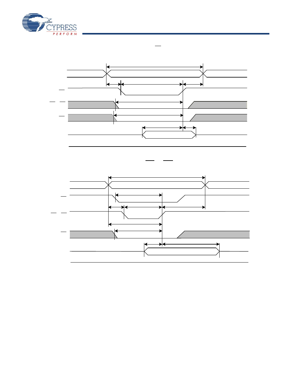
Figure 9. SRAM Write Cycle #2: CE Controlled
Figure 10. SRAM Write Cycle #3: BHE and BLE Controlled
Data Output
Data Input
Input Data Valid
High Impedance
Address Valid
Address
t
WC
t
SD
t
HD
BHE, BLE
WE
CE
t
SA
t
SCE
t
HA
t
BW
t
PWE
'DWD2XWSXW
'DWD,QSXW
,QSXW'DWD9DOLG
+LJK,PSHGDQFH
$GGUHVV9DOLG
$GGUHVV
W
:&
W
6'
W
+'
%+(%/(
:(
&(
W
6&(
W
6$
W
%:
W
+$
W
$:
W
3:(
This manual is related to the following products:
See also other documents in the category Cypress Hardware:
- CY7C1410AV18 (29 pages)
- CY7C1411JV18 (28 pages)
- CY7C1383FV25 (28 pages)
- CY14B256L (18 pages)
- CY7C1307BV25 (21 pages)
- CY7C1041DV33 (13 pages)
- CY62167EV18 (13 pages)
- Perform CY7C1565V18 (28 pages)
- STK11C68-5 (15 pages)
- 7C185-20 (11 pages)
- CY7C1168V18 (27 pages)
- CY7C1318CV18-250BZC (26 pages)
- CY7C1364C (18 pages)
- Perform CY7C1382D (34 pages)
- CY7C106D (11 pages)
- CY14E102N (21 pages)
- CY7C1418AV18 (31 pages)
- enCoRe CY7C638xx (83 pages)
- CY7C1018DV33 (9 pages)
- CY7C1292DV18 (23 pages)
- CY7C130 (19 pages)
- CY7C1424BV18 (30 pages)
- CY62157EV18 (12 pages)
- CY7C1392BV18 (31 pages)
- CY7C1302DV25 (18 pages)
- Perform CY7C1511KV18 (31 pages)
- West Bridge Astoria AN46860 (4 pages)
- CY7C1386FV25 (30 pages)
- CY7C1163V18 (29 pages)
- CY7C1266V18 (27 pages)
- CY7C1334H (13 pages)
- CY7C1018CV33 (7 pages)
- CY62136VN (12 pages)
- AN20639 (3 pages)
- CY7C1338G (17 pages)
- CY7C1462AV33 (27 pages)
- CY7C1145V18 (28 pages)
- STK11C88 (15 pages)
- CY7C1231H (12 pages)
- Perform CY7C142 (15 pages)
- CY14E256L (18 pages)
- STK15C88 (15 pages)
- CY7C1297H (15 pages)
- CY7C1441AV33 (31 pages)
- CapSense CY8C20x36 (34 pages)