Selection guide, Pin configuration – Cypress CY7C1041DV33 User Manual
Page 2
CY7C1041DV33
Document #: 38-05473 Rev. *E
Page 2 of 13
Selection Guide
Description
–10 (Industrial)
–12 (Automotive)
[2]
Unit
Maximum Access Time
10
12
ns
Maximum Operating Current
90
95
mA
Maximum CMOS Standby Current
10
15
mA
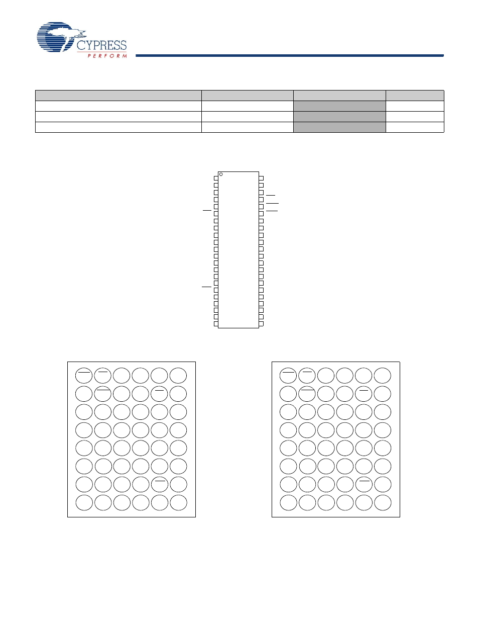
Pin Configuration
Figure 1. 44-Pin SOJ/TSOP II
Figure 2. 48-Ball VFBGA (Pinout 1)
Figure 3. 48-Ball VFBGA (Pinout 2)
1
2
3
4
5
6
7
8
9
11
14
31
32
36
35
34
33
37
40
39
38
12
13
41
44
43
42
16
15
29
30
A
17
18
17
20
19
27
28
25
26
22
21
23
24
A
16
A
15
A
0
A
1
A
2
A
3
A
4
A
7
A
6
A
14
A
13
A
12
A
11
A
9
A
8
A
10
OE
BHE
BLE
CE
WE
IO
0
IO
1
IO
2
IO
3
IO
4
IO
5
IO
6
IO
7
IO
8
IO
9
IO
10
IO
11
IO
12
IO
13
IO
14
IO
15
V
CC
V
CC
V
SS
V
SS
NC
10
A
5
WE
V
CC
A
11
A
10
NC
A
6
A
0
A
3
CE
IO
2
IO
0
IO
1
A
4
A
5
IO
3
IO
5
IO
4
IO
6
IO
7
V
SS
A
9
A
8
OE
V
SS
A
7
IO
8
BHE
NC
A
17
A
2
A
1
BLE
V
CC
IO
9
IO
10
IO
11
IO
12
IO
13
IO
14
IO
15
A
15
A
14
A
13
A
12
NC
NC
NC
3
2
6
5
4
1
D
E
B
A
C
F
G
H
A
16
WE
V
CC
A
11
A
10
NC
A
6
A
0
A
3
CE
IO
10
IO
8
IO
9
A
4
A
5
IO
11
IO
13
IO
12
IO
14
IO
15
V
SS
A
9
A
8
OE
V
SS
A
7
IO
0
BHE
NC
A
17
A
2
A
1
BLE
V
CC
IO
2
IO
1
IO
3
IO
4
IO
5
IO
6
IO
7
A
15
A
14
A
13
A
12
NC
NC
NC
3
2
6
5
4
1
D
E
B
A
C
F
G
H
A
16
Notes
2. Automotive product information is Preliminary.
3. NC pins are not connected on the die.
4. Pinout 1 is compliant with CY7C1041CV33 and pinout 2 is JEDEC compliant. The difference between the two is that the higher and lower byte IOs (IO
[7:0]
and IO
[15:8]
balls) are swapped.