Vicor PFC Micro Power Factor Corrected AC-DC Switcher User Manual
Page 11

03-000048 rev A
Vicor 800-735-6200 Westcor Division 408-522-5280 Applications Engineering 800-927-9474 Pg. 11
PFC Micro Design Guide
User Interface Connections
Signal Ground (CBJ3-1)
Signal Ground on CBJ3-1 is an isolated secondary ground reference for all CBJ3 interfacing signals. This is not
the same as Earth Ground on input power connector MBJ1.
Bi -directional I/O lines (CBJ3-4 to CBJ3-9) (Enable/Disable or Module Power Good Status)
Enable/Disable Mode
Enable/Disable mode is the default condition for these I/O lines. In this mode, the control pins allow the outputs
to be sequenced either ON or OFF. To disable a module, the E/D pin should be pulled low to less than 0.7V with
respect to Signal Ground. The E/D lines will typically source 250
μA (1mA max.) under this condition. To enable
a module, a E/D pin should be open circuited or driven high to a logic high voltage of 3.5V (40
μA typical) or
greater not to exceed 5V. (When one has a two module array, use GSD to disable the output instead of using E/D.)
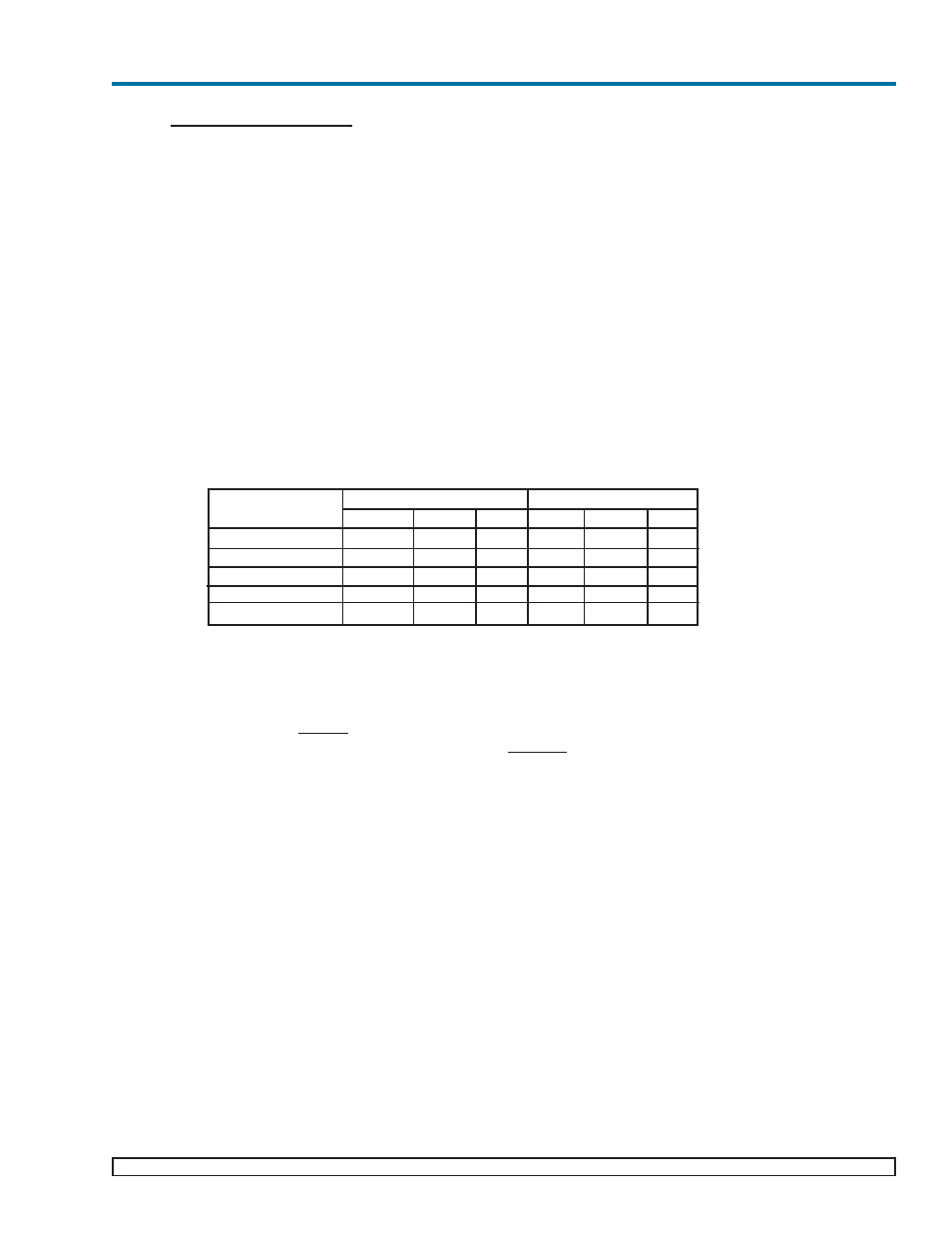
The correspondence between a module and its E/D line as seen from the output end of the power supply goes from
left to right. The PFC Micro Power Supply is a two slot box. Slot 1 is the left slot and Slot 2 is the right slot. See
Table 1. E/D1, E/D2, E/D3 correspond with Vout M1, Vout M2 and Vout M3 on slot 1. E/D4, E/D5, E/D6 cor-
respond with Vout M1, Vout M2 and Vout M3 on slot 2.
Table 1: Enable/Disable Mode
Module Power Good Status Mode
The power supply will enter the Power Good Status Mode when logic high (50mA typical) is applied to Power
Good Read (PGR) pin (CBJ3-2). After transitioning to PGR mode the I/O lines (CBJ3-4 to CBJ3-9) will be out-
puts and will give a onetime readout of the associated module status.. These outputs give an indication of the sta-
tus of the modules of the power supply at the time of transition to PGR. A TTL "1" (>3.5V) on a line indicates the
module is ON and functioning properly, and a TTL "0" (<0.7V) indicates the module is either OFF or is not func-
tioning properly. The correspondence between the module and the Power Good Status of that module is the same
as between a E/D pin and its module. This mode does NOT constantly monitor the module status and must be re-
triggered by transitioning the PGR pin from logic low to logic high to get current module status
Procedurally, certain guidelines must be followed when using this feature. Upon application of a logic high on the
Power Good Read (PGR) pin, the user must change its E/D interface (CBJ3-4 to CBJ3-9) from outputs to inputs
within 3 ms. The Power Good Status data will be valid on the E/D lines when the Power Good Data Valid (PGDV)
pin (CBJ3-11) asserts to a logic high. The power good status measurement takes typically 200ms. While in the
Power Good Read Mode (PGR=1) the individual shutdown lines are not functional. However, General Shut Down
(GSD) is functional. Leaving the Power Good Read mode is accomplished by removing the logic high or applying
a logic low (<0.7V) to the Power Good Read (PGR) pin (CBJ3-2). The user must change its E/D interface (CBJ3-
4 to CBJ3-9) from inputs to outputs between 1ms and 4ms of the time the PGR low is applied to pin CBJ3-2.
Note: If any model is disabled by the user when a Power Good Read is requested (PGR=1), that module will
remain off during the Power Good Read and status of said module will be power not good (<0.7V). Power Good
Read status data on open E/D lines are not valid. An open E/D line is a E/D pin where there is no module associ-
ated with said E/D line (i.e. A power supply with two Maxi modules, Data on E/D2, E/D3 and E/D5 and E/D6 are
NOT valid.
The Power Good Status Mode feature is only valid when Maxi, Mini and/or Micro modules are used.
The following page shows examples of triggering PGR with a 1Hz square while monitoring PGDV and a selected
E/D line with a good module and a defective one
Slot 1
Slot 2
E/D1
E/D2
E/D3
E/D4
E/D5
E/D6
Maxi Modules
X
X
Mini Modules
X
X
X
X
Micro Modules
X
X
X
X
X
X
VI-200 Modules
X
X
VI-J00 Modules
X
X
X
X
