BNC 6040 User Manual
Page 53
53
THEORY OF OPERATION
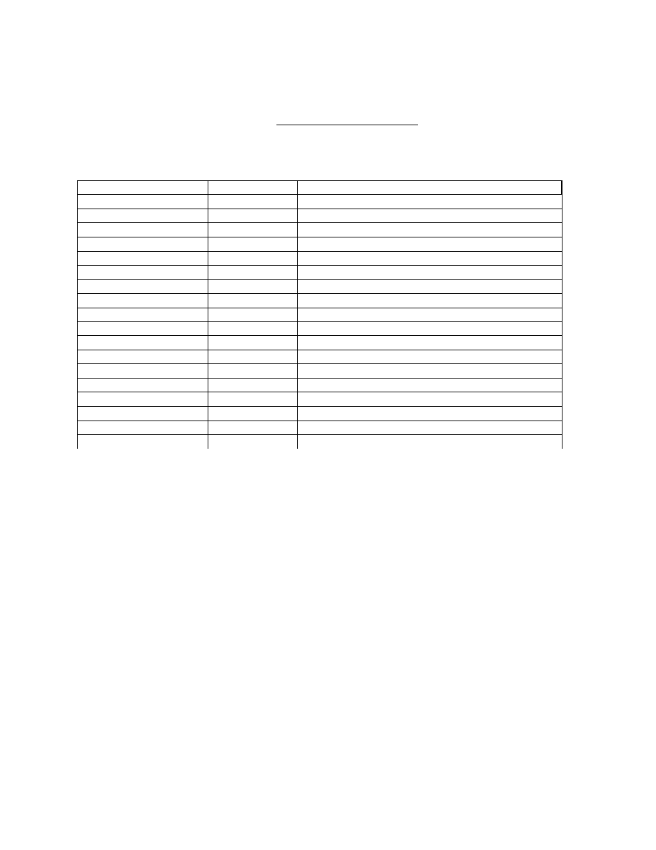
Table 1-9. J9, Microprocessor to ECL Interface Signals
Signal
Pin Number
Description
PLLVAR
14
PLL variable frequency
FTTL1
16
Output of first CMOS frequency divider
FTTL2
17
Output of second CMOS frequency divider
PLLIN
15
VCO input
PLLREF
20
PLL reference frequency
RTLMTTR
19
Rate Limit trigger
RLMTHD
18
Rate Limit Hold signal
ELDCLK
1
ECL Timing count chain, load clock
ELDEN
3
ECL Timing count chain, enable load
DTTLCK
7
Delay time base
DHLDOFF
9
Disables triggering of ECL Delay
DTTLEN
4
Enables ECL Delay to generate DTTLCK
DTTLCOIN
10
CMOS Delay count is at zero
WTTLCK
5
Width time base
WHLWOFF
6
Disables triggering of ECL Width
WTTLEN
2
Enables ECL Width to generate WTTLCK
WTTLCOIN
8
CMOS Width count is at zero
11, 12, 13
Unused
The VCO is operated over the frequency range of 80 to 160 MHz. This is divided by 16 and level shifted
to produce the signal PLLIN (a CMOS signal with a frequency between 5 and 10 MHz). The PLLIN
feeds two counters, Z23-A and Z23-B. Z23-A generates the PLLVAR signal. Z23-B produces the
FTTL1 signal and also clocks Z23-C, which generates the FTTL2 signal. The counter Z27-A, is clocked
from the 10 MHz crystal oscillator, and produces the PLLREF signal, a fixed frequency of 500 Hz. This
is used by the PLL for the reference frequency, and the PLL adjusts the VCO to force the PLLVAR
signal to the same frequency.
Rate Limit:
Z27-B is used to prevent external triggering above certain frequencies. The counter is triggered by the
signal RTLMTTR, and triggers are ignored until the output RLMTHD returns low. This is used with
certain plug-in modules that have upper frequency limits below 100 MHz.
Loading ECL Count Chain:
The signals ELDEN and ELDCLK are used to enable and load new data into the ECL Timing
counters, Z6 and Z28, (PCS 6040-3, schematic 6040-32, sheets 2 and 3).
CMOS to ECL Timing Interface signals:
Please refer to the CMOS Width and Delay Circuits for a description of these signals.