BNC 6040 User Manual
Page 52
52
THEORY OF OPERATION
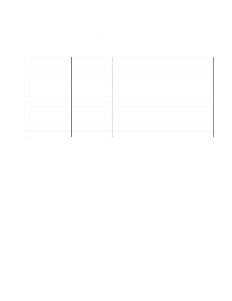
Table 1-8. J8, Microprocessor to Module Interface Signals
Signal(s)
Pin Number
Description
QAD0-QAD7
8-1
8 multiplexed data/address lines
QA8-QA12
16-12
5 address lines
QRD
11
Module read
QWR
10
Module write
QALE
9
Address Latch Enable (demux QAD0-QAD07)
PLUGIN
18
Enables Module interface circuits
RESET
17
System reset
MOD DIS
19
Disables Module
+5
26, 28
+5 V supply
-5.2 V
34, 36
-5.2 V supply
+12 V
37, 39
12 V supply
-12 v
38, 40
-12 V supply
THE
27
+3 V supply
GND
35, 29-33
Ground
20-25
Unused
PLL Synthesizer:
The 6040's internal trigger generator is made of two subsections. The VCO. loop fillers, and range
selection circuits are located on the timing board (PCB 6040-2). The 82C54 CMOS dividers are located
on the microprocessor board (PCB 6040-3).