Pin descriptions, Cs5581 – Cirrus Logic CS5581 User Manual
Page 28
CS5581
28
DS796PP1
3/26/08
10:50
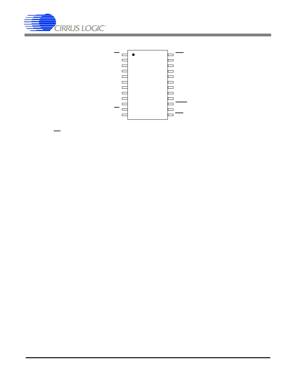
4. PIN DESCRIPTIONS
CS – Chip Select, Pin 1
The Chip Select pin allows an external device to access the serial port. When held high, the
SDO output will be held in a high-impedance output state.
TST – Factory Test, Pin 2
For factory use only. Connect to VLR.
SMODE – Serial Mode Select, Pin 3
The serial interface mode pin (SMODE) dictates whether the serial port behaves as a master or
slave interface. If SMODE is tied high (to VL), the port will operate in the Synchronous
Self-Clocking (SSC) mode. In SSC mode, the port acts as a master in which the converter out-
puts both the SDO and SCLK signals. If SMODE is tied low (to VLR), the port will operate in the
Synchronous External Clocking (SEC) mode. In SEC mode, the port acts as a slave in which
the external logic or microcontroller generates the SCLK used to output the conversion data
word from the SDO pin.
AIN – Analog Input, Pin 4
AIN is the single-ended input.
ACOM – Analog Return, Pin 5
ACOM is the analog return for the input signal.
V1- – Negative Power 1, Pin 6
The V1- and V2- pins provide a negative supply voltage to the core circuitry of the chip. These
two pins should be decoupled as shown in the application block diagrams. V1- and V2- should
be supplied from the same source voltage. For single-supply operation, these two voltages are
nominally 0 V (Ground). For dual-supply, operation they are nominally -2.5 V.
V1+ – Positive Power 1, Pin 7
The V1+ and V2+ pins provide a positive supply voltage to the core circuitry of the chip. These
two pins should be decoupled as shown in the application block diagrams. V1+ and V2+ should
be supplied from the same source voltage. For single-supply operation, these two voltages are
nominally +5 V. For dual-supply operation, they are nominally +2.5 V.
BUFEN – Buffer Enable, Pin 8
Buffers on input pins AIN and ACOM are enabled if BUFEN is connected to V1+ and disabled if
connected to V1-.
VREF+, VREF- – Voltage Reference Input, Pins 9, 10
A differential voltage reference input on these pins functions as the voltage reference for the
converter. The voltage between these pins can range between 2.4 volts and 4.2 volts, with
4.096 volts being the nominal reference voltage value.
RST
Reset
VLR3
Logic Interface Return 3
CONV
Convert
DCR
Digital Core Regulator
V2+
Positive Voltage 2
V2-
Negative Voltage 2
MCLK
Master Clock
VLR
Logic Interface Return
VL
Logic Interface Power
SDO
Serial Data Output
SCLK
Serial Clock Input/Output
RDY
Ready
VLR2
Logic Interface Return 2
BP/UP
Bipolar/Unipolar Select
VREF-
Voltage Reference Input
VREF+
Voltage Reference Input
BUFEN
Buffer Enable
V1+
Positive Power 1
V1-
Negative Power 1
ACOM
Analog Return
AIN
Analog Input
CS
Chip Select
TST
Factory Test
SMODE
Serial Mode Select
12
11
10
9
8
7
6
5
4
3
2
1
13
14
15
16
17
18
19
20
21
22
23
24