3 voltage reference, 4 analog input, 3 voltage reference 3.4 analog input – Cirrus Logic CS5581 User Manual
Page 15: Figure 5. voltage reference circuit, Cs5581
CS5581
DS796PP1
15
3/25/08
14:34
3.3 Voltage Reference
The voltage reference for the CS5581 can range from 2.4 volt to 4.2 volts. A 4.096 volt reference is re-
quired to achieve the specified signal-to-noise performance.
and
illustrate the connec-
tion of the voltage reference with either a single +5 V analog supply or with ±2.5 V.
For optimum performance, the voltage reference device should be one that provides a capacitor connec-
tion to provide a means of noise filtering, or the output should include some type of bandwidth-limiting fil-
ter.
Some 4.096 volt reference devices need only 5 volts total supply for operation and can be connected as
shown in
. The reference should have a local bypass capacitor and an appropriate
output capacitor.
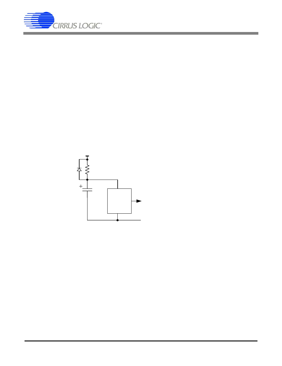
Some older 4.096 voltage reference designs require more headroom and must operate from an input volt-
age of 5.5 to 6.5 volts. If this type of voltage reference is used ensure that when power is applied to the
system, the voltage reference rise time is slower than the rise time of the V1+ and V1- power supply volt-
age to the converter. An example circuit to slow the output startup time of the reference is illustrated in
Figure 5. Voltage Reference Circuit
3.4 Analog Input
The analog input of the converter is single-ended with a full-scale input of
±
2.048 volts, relative to the
ACOM pin. This is illustrated in
. These diagrams also illustrate a differential buffer
amplifier configuration for driving the CS5581.
The capacitors at the outputs of the amplifiers provide a charge reservoir for the dynamic current from the
A/D inputs while the resistors isolate the dynamic current from the amplifier. The amplifiers can be pow-
ered from higher supplies than those used by the A/D but precautions should be taken to ensure that the
op amp output voltage remains within the power supply limits of the A/D, especially under start-up condi-
tions.
2k
10
µF
5.5 to 15 V
VIN
VOUT
GND
4.096 V
Refer to V1- and VREF1 pins.