6 typical connection diagrams, Figure 6, Shown in – Cirrus Logic CS5581 User Manual
Page 17: Ed in, Cs5581
CS5581
DS796PP1
17
3/25/08
14:34
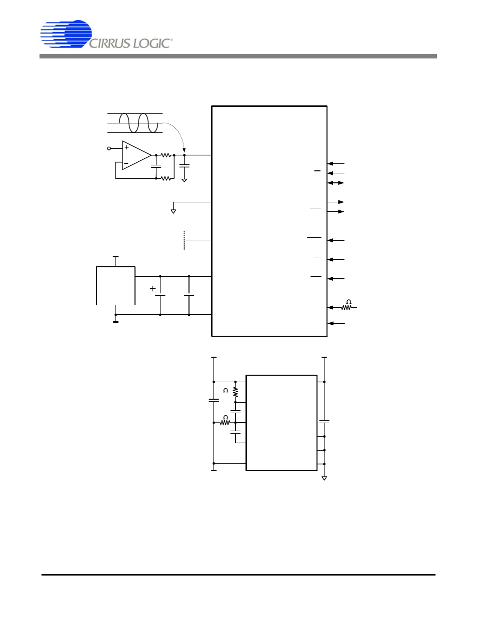
3.6 Typical Connection Diagrams
The following figure depicts the CS5581 powered from bipolar analog supplies, +2.5 V and - 2.5 V.
Figure 6. CS5581 Configured Using
±2.5V Analog Supplies
VREF-
VREF+
+4.096
Voltage
Reference
(NOTE 1)
ACOM
AIN
+2.5 V
SMODE
CS
5
SCLK
5
SDO
RDY
CONV
MCLK
RST
BP/UP
1. See Section 3.3 Voltage Reference for information on required
voltage reference performance criteria.
2.Locate capacitors so as to minimize loop length.
3. The ±2.5 V supplies should also be bypassed to ground at the converter.
4. VLR and the power supply ground for the ±2.5 V should be
connected to the same ground plane under the chip.
5. SCLK and SDO may require pull-down resistors in some applications.
NOTES
-2.5 V
BUFEN
(V-) Buffers Off
(V+) Buffers On
10 µF
0.1 µF
V1+
V2+
V1-
V2-
VL
VLR
DCR
+2.5 V
+3.3 V to +1.8 V
0.1 µF
0.1 µF
X7R
0.1 µF
10
49.9
150pF
2k
4700pF
C0G
-2.048 V
+2.048 V
0 V
-2.5 V
CS5571
TST
10
0.1 µF
VLR2
50
VLR3
CS3003
CS5581
- CobraNet (147 pages)
- CS4961xx (54 pages)
- CS150x (8 pages)
- CS1501 (16 pages)
- CS1601 (2 pages)
- CS1601 (16 pages)
- CS1610 (16 pages)
- CRD1610-8W (24 pages)
- CRD1611-8W (25 pages)
- CDB1610-8W (21 pages)
- CS1610A (18 pages)
- CDB1611-8W (21 pages)
- CDB1610A-8W (21 pages)
- CDB1611A-8W (21 pages)
- CRD1610A-8W (24 pages)
- CRD1611A-8W (25 pages)
- CS1615 (16 pages)
- AN403 (15 pages)
- AN401 (14 pages)
- AN400 (15 pages)
- AN375 (27 pages)
- AN376 (9 pages)
- CRD1615-8W (22 pages)
- CRD1616-8W (23 pages)
- AN402 (14 pages)
- AN404 (15 pages)
- CRD1615A-8W (21 pages)
- CS1615A (16 pages)
- CS1630 (56 pages)
- AN374 (35 pages)
- AN368 (80 pages)
- CRD1630-10W (24 pages)
- CRD1631-10W (25 pages)
- CS1680 (16 pages)
- AN405 (13 pages)
- AN379 (31 pages)
- CRD1680-7W (31 pages)
- AN335 (10 pages)
- AN334 (6 pages)
- AN312 (14 pages)
- AN Integrating CobraNet into Audio Products (16 pages)
- CobraNet Audio Routing Primer (9 pages)
- Bundle Assignments in CobraNet Systems (3 pages)
- CS2300-01 (3 pages)
- CS2000-CP (38 pages)