Cirrus Logic CS5581 User Manual
Cs5581, Preliminary product information, Features & description
Preliminary Product Information
This document contains information for a new product.
Cirrus Logic reserves the right to modify this product without notice.
Copyright
© Cirrus Logic, Inc. 2008
(All Rights Reserved)
3/25/08
15:11
CS5581
±
2.5 V / 5 V, 200 kSps, 16-bit, High-throughput
∆Σ
ADC
Features
& Description
Single-ended Analog Input
On-chip Buffers for High Input Impedance
Conversion Time = 5
µS
Settles in One Conversion
Linearity Error = 0.0008%
Signal-to-Noise = 80 dB
S/(N + D) = 80 dB
DNL = ±0.1 LSB Max.
Simple three/four-wire serial interface
Power Supply Configurations:
- Analog: +5V/GND; IO: +1.8V to +3.3V
- Analog: ±2.5V; IO: +1.8V to +3.3V
Power Consumption:
- ADC Input Buffers On: 85 mW
- ADC Input Buffers Off: 60 mW
General Description
The CS5581 is a single-channel, 16-bit analog-to-digital
converter capable of 200 kSps conversion rate. The input
accepts a single-ended analog input signal. On-chip buff-
ers provide high input impedance for both the AIN input
and the VREF+ input. This significantly reduces the drive
requirements of signal sources and reduces errors due to
source impedances. The CS5581 is a delta-sigma convert-
er capable of switching multiple input channels at a high
rate with no loss in throughput. The ADC uses a low-laten-
cy digital filter architecture. The filter is designed for fast
settling and settles to full accuracy in one conversion. The
converter's 16-bit data output is in serial format, with the
serial port acting as either a master or a slave. The convert-
er is designed to support bipolar, ground-referenced
signals when operated from ±2.5V analog supplies.
The converter can operate from an analog supply of 0-5V
or from ±2.5V. The digital interface supports standard logic
operating from 1.8, 2.5, or 3.3 V.
ORDERING INFORMATION:
See
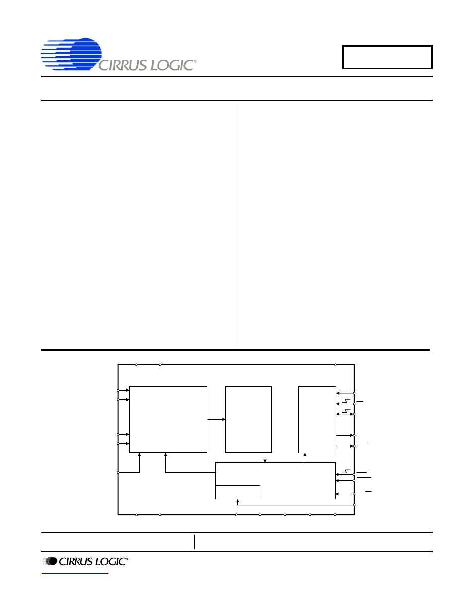
AIN
ACOM
CS
SCLK
SMODE
VREF+
VREF-
RDY
OSC/CLOCK
GENERATOR
CONV
BP/UP
DIGITAL CONTROL
SERIAL
INTERFACE
ADC
DIGITAL
FILTER
LOGIC
VL
MCLK
SDO
RST
DCR
VLR
V1-
V2-
BUFEN
V2+
V1+
CS5581
TST
VLR2
VLR3
MAR ‘08
DS796PP1
Document Outline
- Features & Description
- General Description
- Table of Contents
- List of Figures
- List of Tables
- 1. Characteristics and Specifications
- 2. Overview
- 3. Theory of Operation
- 3.1 Converter Operation
- 3.2 Clock
- 3.3 Voltage Reference
- 3.4 Analog Input
- 3.5 Output Coding Format
- 3.6 Typical Connection Diagrams
- 3.7 AIN & VREF Sampling Structures
- 3.8 Converter Performance
- 3.9 Digital Filter Characteristics
- 3.10 Serial Port
- 3.11 Power Supplies & Grounding
- 3.12 Using the CS5581 in Multiplexing Applications
- 3.13 Synchronizing Multiple Converters
- 4. Pin Descriptions
- 5. Package Dimensions
- 6. Ordering Information
- 7. Environmental, Manufacturing, & Handling Information
- 8. Revision History