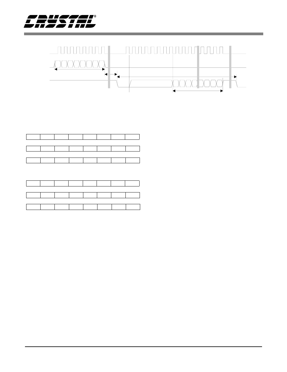
Figure 5. conversion/acquisition cycle timing, Development tool description, Conclusion – Cirrus Logic AN130 User Manual
Page 5: Development tool description 7. conclusion, An130

AN130
AN130REV2
5
for a selectable clock polarity. However, many do
not have the capability to select the clock’s phase.
When using a microcontroller with both features,
the clock polarity should be set to idle low, and the
clock phase should be set to begin clocking in the
middle of the data bits. For an SPI port without the
variable clock phase feature to function properly
with the CS5521/22/23/24/28, the clock polarity
needs to be set to idle high, and the ADC’s serial
port must be re-initialized anytime new informa-
tion is transmitted between the microcontroller and
the converter.
6. DEVELOPMENT TOOL
DESCRIPTION
The code in this application note was developed
with MPLAB
TM
, a development package from Mi-
crochip, Inc. It was written in Microchip assembly
and compiled with the MPASM
TM
assembler.
7. CONCLUSION
This application note presents an example of how
to interface the CS5521/22/23/24/28 to the
PIC16C84. It is divided into two main sections:
hardware and software. The hardware section illus-
trates both a three-wire and a four-wire interface.
The three-wire interface is SPI™ and MICROW-
IRE™ compatible. The software, developed using
tools from Microchip, Inc., illustrates how to ini-
tialize the converter and microcontroller, write to
the CSRs, write and read the ADC’s internal regis-
ters, perform calibrations, and acquire conversions.
The software is modularized and provides impor-
tant subroutines such as write_register,
read_register,
write_csrs and convert, which were
all written in PIC assembly language.
The software described in the note is included in
Section 8. “APPENDIX: PIC16C84 Microcode to
Interface to the CS5521/22/23/24/28” on page 6.
Command Time
8 SCLKs
8 SCLKs Clear SDO Flag
Data SDO Continuous Conversion Read
SDO
SCLK
SDI
t *
d
Data Time
24 SCLKs
MSB
LSB
* td = XIN/OWR clock cycles for each conversion except the
first conversion which will take XIN/OWR + 7 clock cycles
XIN/OWR
Clock Cycles
Figure 5. Conversion/Acquisition Cycle Timing
MSB
High-Byte
Mid-Byte
Low-ByteLSB
A) 24-Bit Conversion Data Word (CS5522/24/28)
MSB
High-Byte
Mid-Byte
Low-Byte
B) 16-bit Conversion Data Word (CS5521/23)
0 - always zero, 1 - always 1
CI1, CI0 - Channel Indicator Bits
OD - Oscillation Detect, OF - Overflow
D23
D22
D21
D20
D19
D18
D17
D16
D15
D14
D13
D12
D11
D10
D9
D8
D7
D6
D5
D4
D3
D2
D1
D0
D15
D14
D13
D12
D11
D10
D9
D8
D7
D6
D5
D4
D3
D2
D1
D0
1
1
1
0
CI1
CI0
OD
OF
Figure 6. Bit Representation/Storage in the PIC16C84
