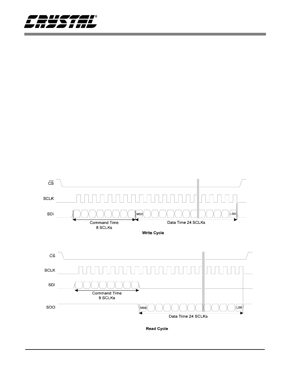
5 acquire conversion, Figure 3. write-cycle timing, Figure 4. read-cycle timing – Cirrus Logic AN130 User Manual
Page 4: Maximum sclk rate, Serial peripheral interface, Maximum sclk rate 5. serial peripheral interface, An130

AN130
4
AN130REV2
3.5 Acquire Conversion
To acquire a conversion the subroutine convert is
called. For single conversions on one physical
channel, the MC (multiple conversion) and the LP
(loop) bits in the configuration register must be log-
ic 0. To prevent corruption of the configuration
register, convert instructs the PIC16C84 to read
and save the contents. This information is stored in
the variables HIGHBYTE, MIDBYTE and LOW-
BYTE. Then the MC, LP, and RC (read convert)
bits are masked to logic 0, and the new information
is written back to the ADC’s configuration register.
A conversion is initiated on Setup 1 by sending the
command 0x80 to the converter. At this time, the
controller polls RA2 (SDO) until it falls to a logic
0 level (see Figure 5). After SDO falls, convert ap-
plies a logic 0 to RA1 (SDI) and pulses RA3
(SCLK) eight times to initiate the data transfer
from the ADC. The PIC16C84 then reads the con-
version data word by calling receive_byte three
times. Figure 6 depicts how the 16 or 24-bit data
word is stored in the memory locations HIGH-
BYTE, MIDBYTE, and LOWBYTE.
4. MAXIMUM SCLK RATE
An instruction cycle in the PIC16C84 consists of
four oscillator periods, or 400ns if the microcon-
troller’s oscillator frequency is 10 MHz. Since the
CS5521/22/23/24/28’s maximum SCLK rate is
2MHz, additional no operation (NOP) delays may
be necessary to reduce the transfer rate if the micro-
controller system requires higher rate oscillators.
5. SERIAL PERIPHERAL INTERFACE
When using a built-in Serial Peripheral Interface
(SPI) port, the designer must pay special attention
to how the port is configured. Most SPI ports allow
Figure 3. Write-Cycle Timing
Figure 4. Read-Cycle Timing
