Cirrus Logic CS5464 User Manual
Cs5464 three-channel, single-phase power/energy ic
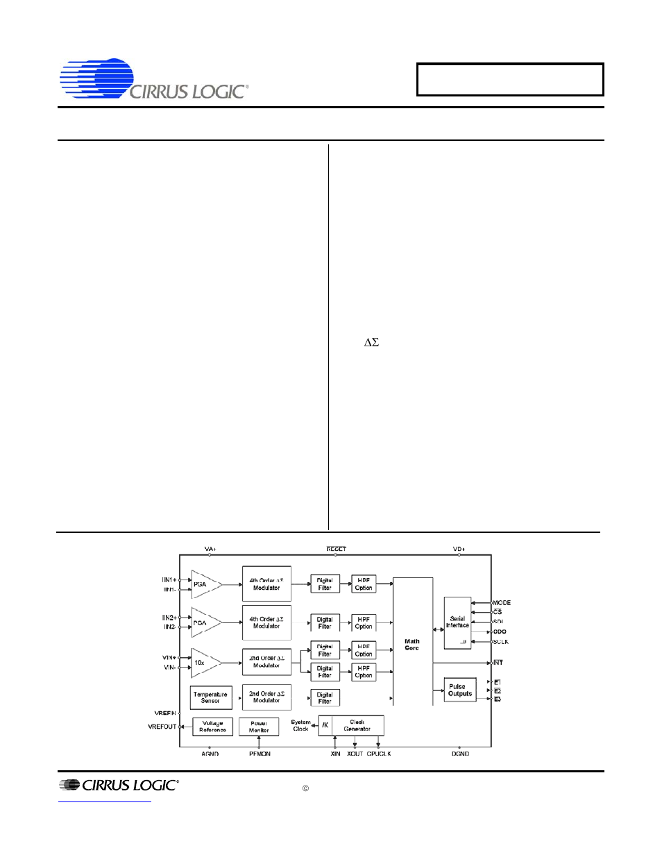
Table of contents
Document Outline
- Features & Description
- 1. Overview
- 2. Pin Description
- 3. Characteristics & Specifications
- 4. Signal Path Description
- 5. Pin Descriptions
- 6. Setting Up the CS5464
- 6.1 Clock Divider
- 6.2 CPU Clock Inversion
- 6.3 Interrupt Pin Behavior
- 6.4 Current Input Gain Ranges
- 6.5 High-pass Filters
- 6.6 Cycle Count
- 6.7 Energy Pulse Outputs
- 6.8 No Load Threshold
- 6.9 Energy Pulse Width
- 6.10 Energy Pulse Rate
- 6.11 Voltage Sag/Current Fault Detection
- 6.12 Epsilon
- 6.13 Temperature Measurement
- 7. Using the CS5464
- 8. Register Descriptions
- 8.1 Page Register
- 8.2 Page 0 Registers
- 8.2.1 Configuration (Config) – Address: 0
- 8.2.2 Instantaneous Current (I1, I2), Voltage (V1, V2), and Power (P1, P2)
- 8.2.3 Active Power (P1AVG , P2AVG )
- 8.2.4 RMS Current (I1RMS, I2RMS ) and Voltage (V1RMS, V2RMS )
- 8.2.5 Instantaneous Quadrature Power (Q1, Q2)
- 8.2.6 Reactive Power (Q1AVG, Q2AVG )
- 8.2.7 Peak Current (I1PEAK, I2PEAK ) and Peak Voltage (V1PEAK, V2PEAK )
- 8.2.8 Apparent Power (S1, S2)
- 8.2.9 Power Factor (PF1, PF2)
- 8.2.10 Temperature (T) – Address: 27
- 8.2.11 Active, Apparent, and Reactive Energy Pulse Outputs (EPULSE, SPULSE, QPULSE )
- 8.2.12 Internal Status (Status) and Interrupt Mask (Mask)
- 8.2.13 Control (Ctrl) – Address: 28
- 8.3 Page 1 Registers
- 8.3.1 DC Offset for Current (I1OFF , I2OFF ) and Voltage (V1OFF , V2OFF )
- 8.3.2 Gain for Current (I1GAIN , I2GAIN ) and Voltage (V1GAIN , V2GAIN )
- 8.3.3 Power Offset (P1OFF , P2OFF )
- 8.3.4 AC Offset for Current (I1ACOFF , I2ACOFF ) and Voltage (V1ACOFF , V2ACOFF )
- 8.3.5 Mode Control (Modes) – Address: 16
- 8.3.6 Line to Sample Frequency Ratio (Epsilon) – Address: 17
- 8.3.7 Pulse Output Width (PulseWidth) – Address: 14
- 8.3.8 Pulse Output Rate (PulseRate) – Address: 15
- 8.3.9 Cycle Count (N) – Address: 19
- 8.3.10 Channel Select Level (Ichanlevel ) – Address: 18
- 8.3.11 Channel Select Minimum Amplitude (EMIN or IrmsMIN ) – Address: 24
- 8.3.12 Wideband Reactive Power (Q1WB , Q2WB )
- 8.3.13 Temperature Gain (TGAIN ) – Address: 22
- 8.3.14 Temperature Offset (TOFF ) – Address: 23
- 8.3.15 Filter Settling Time for Conversion Startup (TSETTLE ) – Address: 25
- 8.3.16 No Load Threshold (LoadMIN) – Address 26
- 8.3.17 Voltage Fixed RMS Reference (VFRMS) – Address 27
- 8.3.18 System Gain (G) – Address: 28
- 8.3.19 System Time (Time) – Address: 29
- 8.4 Page 2 Registers
- 9. System Calibration
- 10. E2PROM Operation
- 11. Basic Application Circuits
- 12. Package Dimensions
- 13. Ordering Information
- 14. Environmental, Manufacturing, & Handling Information
- 15. Revision History