Register descriptions, 1 configuration (config) – address: 0, Cs5464 – Cirrus Logic CS5464 User Manual
Page 28: 1 page register, 2 page 0 registers
CS5464
28
DS682F3
8. REGISTER DESCRIPTIONS
1. “Default” = bit states after power-on or reset
2. DO NOT write a “1” to any unpublished register bit.
3. DO NOT write to any unpublished register address.
8.1 Page Register
8.1.1 Page
–
Address: 31, Write-only, can be written from ANY page.
Default = 0
Register Read and Write commands contain only 5 address bits. But the internal address bus of the CS5464 is
12 bits wide. Therefore, registers are organized into “Pages”. There are 128 pages of 32 registers each. The
Page
register provides the 7 high-order address bits and selects one of the 128 register pages. Not all pages
are used,
Page
is a write-only integer containing 7 bits.
8.2 Page 0 Registers
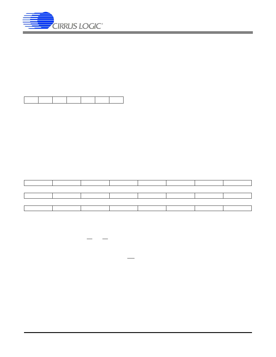
8.2.1 Configuration (Config)
–
Address: 0
Default = 1 (K=1)
PC[7:0]
Phase compensation for channel 1. Sets a delay in voltage, relative to current. Phase is signed
and in the range of -1.0
value 1.0 sample (OWR) intervals.
EWA
Allows the E1 and E2 pins to be configured as open-drain outputs.
0 = Normal Outputs
1 = Open-drain Outputs
IMODE, IINV
Interrupt configuration. Selects INT pin behavior.
00 = Low Logic Level When Asserted
01 = High Logic Level When Asserted
10 = Low-going Pulse on New Interrupt
11 = High-going Pulse on New Interrupt
iCPU
Inverts the CPUCLK output.
0 = Default
1 = Invert CPUCLK.
K[3:0]
Clock divider. Divides MCLK by K to generate internal clock DCLK. (DCLK = MCLK/K). K is
unsigned and in the range of 1 to 16. When zero, K = 16. At reset, K = 1.
MSB
LSB
2
6
2
5
2
4
2
3
2
2
2
1
2
0
23
22
21
20
19
18
17
16
PC7
PC6
PC5
PC4
PC3
PC2
PC1
PC0
15
14
13
12
11
10
9
8
EWA
-
-
IMODE
IINV
-
-
-
7
6
5
4
3
2
1
0
-
-
-
iCPU
K3
K2
K1
K0