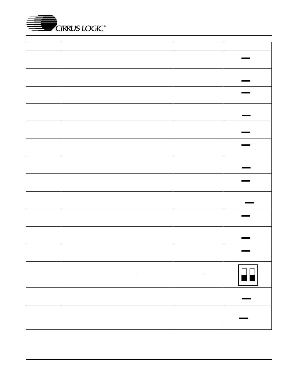
Table 2. default header settings, Cdb5451a, Gain – Cirrus Logic CDB5451A User Manual
Page 6
CDB5451A
6
DS458DB3
Name
Function Description
Default Setting
Default Jumpers
HDR1
Used to switch IIN3+ on the CS5451A between J2
and AGND.
IIN3+ Set to BNC J2
HDR2
Used to switch VIN3- on the CS5451A between J3
and AGND.
VIN3- Set to BNC J3
HDR3
Used to switch VIN3+ on the CS5451A between J1
and AGND.
VIN3- Set to BNC J1
HDR4
Used to switch IIN3- on the CS5451A between J4
and AGND.
IIN3- Set to BNC J4
HDR5
Used to switch VIN2- on the CS5451A between J6
and AGND.
VIN2- Set to BNC J6
HDR6
Used to switch IIN2+ on the CS5451A between J7
and AGND.
IIN2+ Set to BNC J7
HDR7
Used to switch IIN2- on the CS5451A between J5
and AGND.
IIN2+ Set to BNC J5
HDR8
Used to switch VIN2+ on the CS5451A between J8
and AGND.
VIN2+ Set to BNC J8
HDR9
Used to switch between external VA- and on-board
CS5451A charge-pump circuit, CPD
CPD active
HDR10
Used to switch VIN1+ on the CS5451A between J9
and AGND.
VIN1+ Set to BNC J9
HDR11
Used to switch IIN1- on the CS5451A between J12
and AGND.
IIN1- Set to BNC J12
HDR12
Used to switch IIN1+ on the CS5451A between J10
and AGND.
IIN1- Set to BNC J10
SW1
S1-1 sets logic level on CS5451A OWRS input pin
S1-2 sets logic level on CS5451A
GAIN
input pin
SW1-2 Open (XIN/1024)
SW1-1 Open (GAIN=x1)
HDR13
Used to switch VIN1- on the CS5451A between J11
and AGND.
VIN1- Set to BNC J11
HDR14
Used to switch the VREFIN from external VREF
post connector, to the on board LT1004 reference,
or to the on-chip reference VREFOUT. Refer to
Table 3.
VREFIN Set to on-
chip reference
VREFOUT
Table 2. Default Header Settings
O O IIN3+
O O AGND
O O VIN3-
O O AGND
O O VIN3+
O O AGND
O O IIN3-
O O AGND
O O VIN2-
O O AGND
O O IIN2+
O O AGND
O O IIN2-
O O AGND
O O VIN2+
O O AGND
O O
O O
A-
CPD
O O VIN1+
O O AGND
O O IIN1-
O O AGND
O O IIN1+
O O AGND
2
3
OPEN
O O VIN1-
O O AGND
O O LT1004
O O VREFOUT
O O EXT VREF