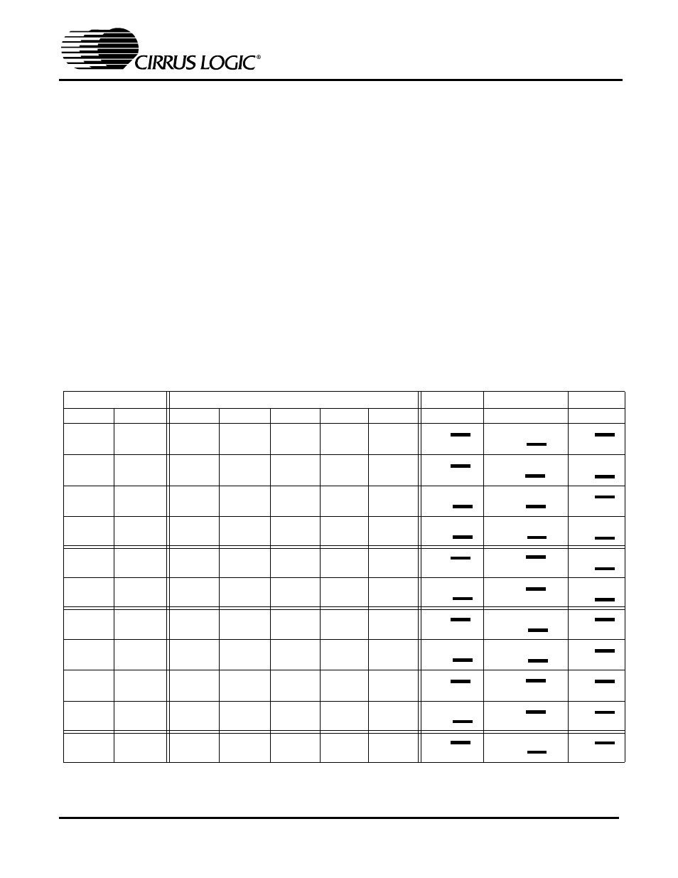
Table 1. power supply connections, 3 charge pump options, 3 eval board control - headers/switches – Cirrus Logic CDB5451A User Manual
Page 5: 1 analog inputs, Cdb5451a

CDB5451A
DS458DB3
5
+5V. This voltage is defined as the voltage pre-
sented across VD+ and DGND.
2.2.3 Charge Pump Options
The output from CS5451A’s charge-pump driver
pin (CPD) can be used to generate a -2V supply
when the proper jumper settings are selected on
HDR9. This -2V supply can be used as the nega-
tive power supply connection for the CS5451A’s
VA- pin. Referring to Figure 1, circuitry for a
charge-pump circuit is included on-board. The
charge pump circuit consists of capacitors C11,
C12, and C36, and diodes D1 and D2.
As an alternative to using the charge pump circuit,
the user can supply an off-board -2V DC power
source to the “A-” banana connector. This option
is controlled by the setting on HDR9.
2.3 Eval Board Control -
Headers/Switches
Table 2 lists the various adjustable headers and
switches on the CDB5451A Evaluation Board, as
well as their default settings (as shipped from the
factory). The header settings can be adjusted by
the user to select various options on the evaluation
board. These options are described further in the
following paragraphs.
2.3.1 Analog Inputs
Refer to Figure 2. The settings on the 12 analog in-
put headers (2 headers per channel) which are
designated as HDR1 up to HDR8, and HDR10 up
to HDR13, determine which inputs will carry a sig-
nal, and which inputs may be grounded. They can
be configured to accept either a single-ended or
Power Supplies
Power Post Connections
Analog
Digital
A+
A-
GND
D+
+5 V_IN
HDR9
HDR17
HDR18
+3
+3
+3
-2
0
+3
NC
+3
+3
+3
-2
0
NC
NC
+3
+3
+3
NC
0
+3
NC
+3
+3
+3
NC
0
NC
NC
+3
+3
NC
-2
0
NC
+5
+3
+3
NC
NC
0
NC
+5
+3
+5
+3
-2
0
+5
NC
+3
+5
+3
NC
0
+5
NC
+3
+5
NC
-2
0
+5
+5
+3
+5
NC
NC
0
+5
+5
+5
+3
+5
0
+2
+5
NC
Table 1. Power Supply Connections
O O
O O
A-
CPD
O O
+5V_IN
A+
O O
O O
O O
VD+
V+
O O
O O
A-
CPD
O O
+5V_IN
A+
O O
O O
O O
VD+
V+
O O
A-
CPD O O
O O
+5V_IN
A+
O O
O O
O O
VD+
V+
O O
A-
CPD O O
O O
+5V_IN
A+
O O
O O
O O
VD+
V+
O O
O O
A-
CPD
O O
+5V_IN
A+
O O
O O
O O
VD+
V+
O O
A-
CPD O O
O O
+5V_IN
A+
O O
O O
O O
VD+
V+
O O
O O
A-
CPD
O O
+5V_IN
A+
O O
O O
O O
VD+
V+
O O
A-
CPD O O
O O
+5V_IN
A+
O O
O O
O O
VD+
V+
O O
O O
A-
CPD
O O
+5V_IN
A+
O O
O O
O O
VD+
V+
O O
A-
CPD O O
O O
+5V_IN
A+
O O
O O
O O
VD+
V+
O O
O O
A-
CPD
O O
+5V_IN
A+
O O
O O
O O
VD+
V+
