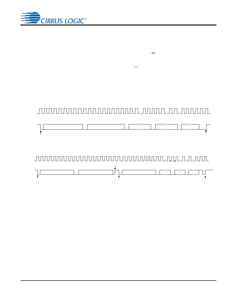
Figure 11. control port timing, i·c write, Figure 12. control port timing, i·c read, Cs5345 – Cirrus Logic CS5345 User Manual
Page 28
28
DS658F4
CS5345
be connected through a resistor to VLC or DGND as desired. The state of the pins is sensed while the
CS5345 is being reset.
The signal timings for a read and write cycle are shown in
. A Start condition is
defined as a falling transition of SDA while the clock is high. A Stop condition is a rising transition while
the clock is high. All other transitions of SDA occur while the clock is low. The first byte sent to the CS5345
after a Start condition consists of a 7-bit chip address field and a R/W bit (high for a read, low for a write).
The upper 5 bits of the 7-bit address field are fixed at 10011. To communicate with a CS5345, the chip
address field, which is the first byte sent to the CS5345, should match 10011 followed by the settings of
the AD1 and AD0. The eighth bit of the address is the R/W bit. If the operation is a write, the next byte is
the Memory Address Pointer (MAP) which selects the register to be read or written. If the operation is a
read, the contents of the register pointed to by the MAP will be output. Following each data byte, the mem-
ory address pointer will automatically increment to facilitate block reads and writes of successive regis-
ters. Each byte is separated by an acknowledge bit. The ACK bit is output from the CS5345 after each
input byte is read, and is input to the CS5345 from the microcontroller after each transmitted byte.
Since the read operation cannot set the MAP, an aborted write operation is used as a preamble. As shown
in
, the write operation is aborted after the acknowledge for the MAP byte by sending a stop con-
dition. The following pseudocode illustrates an aborted write operation followed by a read operation.
Send start condition.
Send 10011xx0 (chip address & write operation).
Receive acknowledge bit.
Send MAP byte.
Receive acknowledge bit.
Send stop condition, aborting write.
Send start condition.
Send 10011xx1 (chip address & read operation).
Receive acknowledge bit.
4 5 6 7
24 25
SCL
CHIP ADDRESS (WRITE)
MAP BYTE
DATA
DATA +1
START
ACK
STOP
ACK
ACK
ACK
1 0 0 1 1 AD1 AD0 0
SDA
6 6 5 4 3 2 1 0
7 6 1 0
7 6 1 0
7 6 1 0
0 1 2 3
8 9
12
16 17 18 19
10 11
13 14 15
27 28
26
DATA +n
Figure 11. Control Port Timing, I²C Write
SCL
CHIP ADDRESS (WRITE)
MAP BYTE
DATA
DATA +1
START
ACK
STOP
ACK
ACK
ACK
1 0 0 1 1 AD1 AD0 0
SDA
1 0 0 1 1 AD1 AD0 1
CHIP ADDRESS (READ)
START
7 6 5 4 3 2 1 0
7 0
7 0
7 0
NO
16
8 9
12 13 14 15
4 5 6 7
0 1
20 21 22 23 24
26 27 28
2 3
10 11
17 18 19
25
ACK
DATA + n
STOP
Figure 12. Control Port Timing, I²C Read