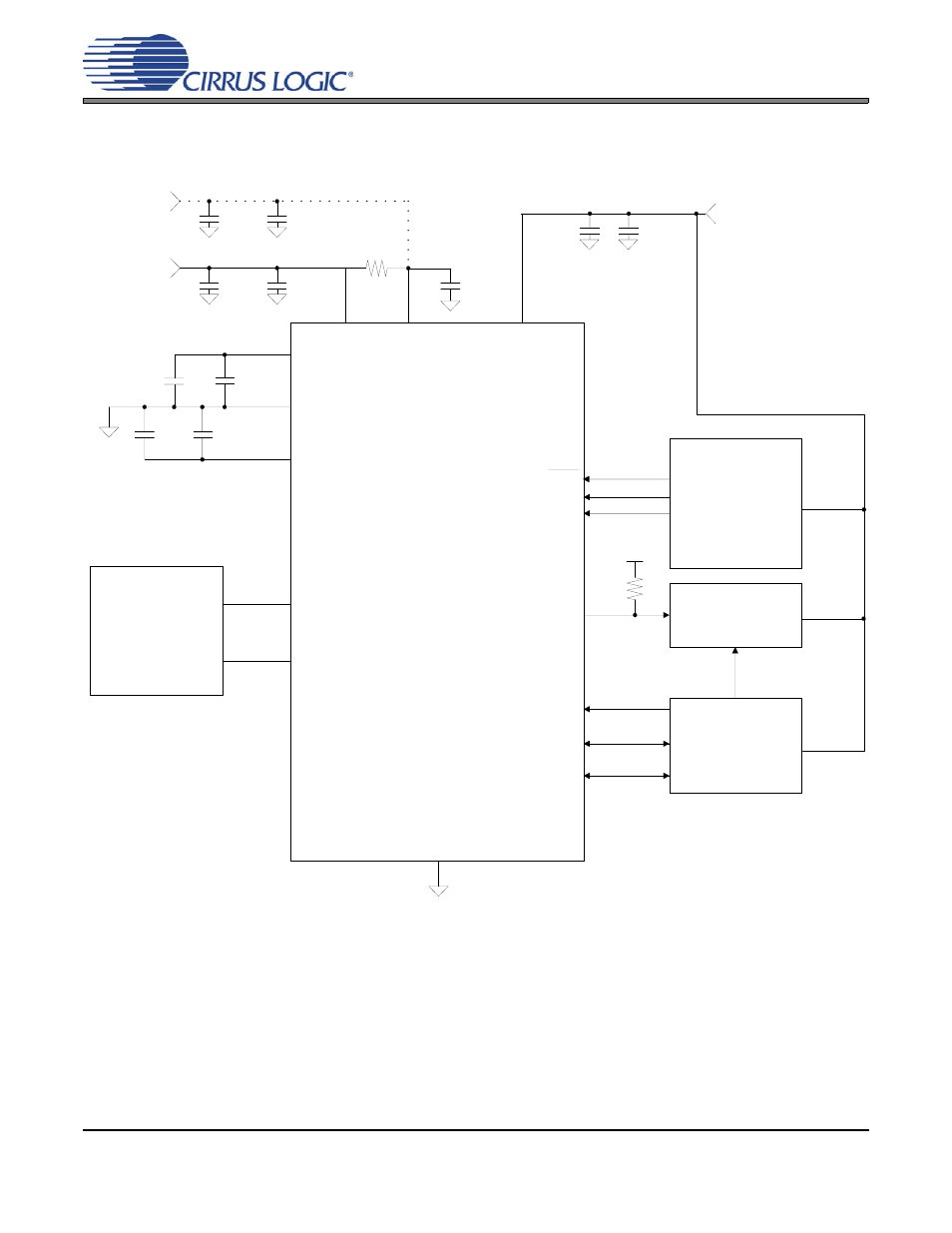
Typical connection diagram – Cirrus Logic CS5341 User Manual
Page 14
14
DS564F2
CS5341
Confidential Draft
3/11/08
3. TYPICAL CONNECTION DIAGRAM
FILT+
V
0.1
µF
A/D CONVERTER
SCLK
CS5341
MCLK
VQ
1
µF
+
RST
VA
L
1
µF
1.8 V to 5V
1
µF
+
+
SDOUT
GND
LRCK
Power Down
and Mode
Settings
Audio Data
Processor
Timing Logic
and Clock
0.1
µF
0.1
µF
0.1
µF
REFGND
1µF
+
AINL
AINR
3.3V to 5V
1
µF
+
0.1
µF
3.3V to 5V
Ω
5.1
V D
0.1
µF
Ω
10k
VL or GND
* Pull-up to VL for I
2
S
Pull-down to GND for LJ
*
M0
M1
Analog Input Buffer
Figure 21
**
** Resistor may only be
used if VD is derived from
VA. If used, do not drive
any other logic from VD
***
*** Capacitor value affects
low frequency distortion
performance as described
in Section 4.8
See also other documents in the category Cirrus Logic Hardware:
- CobraNet (147 pages)
- CS4961xx (54 pages)
- CS150x (8 pages)
- CS1501 (16 pages)
- CS1601 (2 pages)
- CS1601 (16 pages)
- CS1610 (16 pages)
- CRD1610-8W (24 pages)
- CRD1611-8W (25 pages)
- CDB1610-8W (21 pages)
- CS1610A (18 pages)
- CDB1611-8W (21 pages)
- CDB1610A-8W (21 pages)
- CDB1611A-8W (21 pages)
- CRD1610A-8W (24 pages)
- CRD1611A-8W (25 pages)
- CS1615 (16 pages)
- AN403 (15 pages)
- AN401 (14 pages)
- AN400 (15 pages)
- AN375 (27 pages)
- AN376 (9 pages)
- CRD1615-8W (22 pages)
- CRD1616-8W (23 pages)
- AN402 (14 pages)
- AN404 (15 pages)
- CRD1615A-8W (21 pages)
- CS1615A (16 pages)
- CS1630 (56 pages)
- AN374 (35 pages)
- AN368 (80 pages)
- CRD1630-10W (24 pages)
- CRD1631-10W (25 pages)
- CS1680 (16 pages)
- AN405 (13 pages)
- AN379 (31 pages)
- CRD1680-7W (31 pages)
- AN335 (10 pages)
- AN334 (6 pages)
- AN312 (14 pages)
- AN Integrating CobraNet into Audio Products (16 pages)
- CobraNet Audio Routing Primer (9 pages)
- Bundle Assignments in CobraNet Systems (3 pages)
- CS2300-01 (3 pages)
- CS2000-CP (38 pages)