Figure 19. control port timing, i²c write, Figure 20. control port timing, i²c read, Figure 19 – Cirrus Logic CS43L21 User Manual
Page 35: Figure 20, A st, Cs43l21
DS723F1
35
CS43L21
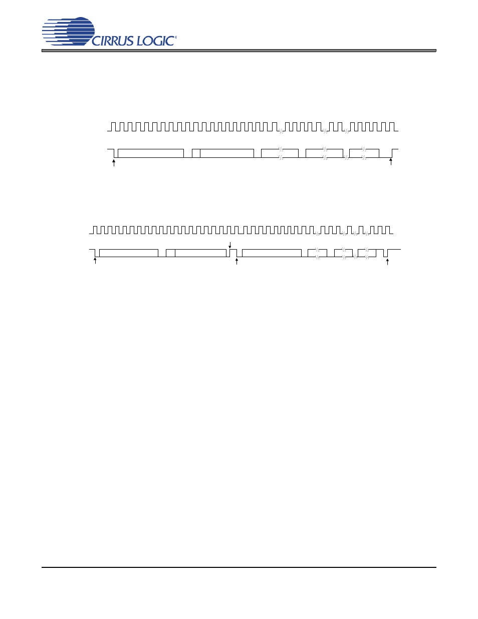
operation is a read, the contents of the register pointed to by the MAP will be output. Setting the auto-
increment bit in MAP allows successive reads or writes of consecutive registers. Each byte is separated
by an acknowledge bit. The ACK bit is output from the CS43L21 after each input byte is read and is input
to the CS43L21 from the microcontroller after each transmitted byte.
Since the read operation cannot set the MAP, an aborted write operation is used as a preamble. As shown
in
, the write operation is aborted after the acknowledge for the MAP byte by sending a stop con-
dition. The following pseudocode illustrates an aborted write operation followed by a read operation.
Send start condition.
Send 100101x0 (chip address & write operation).
Receive acknowledge bit.
Send MAP byte, auto-increment off.
Receive acknowledge bit.
Send stop condition, aborting write.
Send start condition.
Send 100101x1 (chip address & read operation).
Receive acknowledge bit.
Receive byte, contents of selected register.
Send acknowledge bit.
Send stop condition.
Setting the auto-increment bit in the MAP allows successive reads or writes of consecutive registers. Each
byte is separated by an acknowledge bit.
4 5 6 7
24 25
SCL
CHIP ADDRESS (WRITE)
MAP BYTE
DATA
DATA +1
START
ACK
STOP
ACK
ACK
ACK
1 0 0 1 0 1 AD0 0
SDA
INCR
6 5 4 3 2 1 0
7 6 1 0
7 6 1 0
7 6 1 0
0 1 2 3
8 9
12
16 17 18 19
10 11
13 14 15
27 28
26
DATA +n
Figure 19. Control Port Timing, I²C Write
SCL
CHIP ADDRESS (WRITE)
MAP BYTE
DATA
DATA +1
START
ACK
STOP
ACK
ACK
ACK
1 0 0 1 0 1 AD0 0
SDA
1 0 0 1 0 1 AD0 1
CHIP ADDRESS (READ)
START
INCR
6 5 4 3 2 1 0
7 0
7 0
7 0
NO
16
8 9
12 13 14 15
4 5 6 7
0 1
20 21 22 23 24
26 27 28
2 3
10 11
17 18 19
25
ACK
DATA + n
STOP
Figure 20. Control Port Timing, I²C Read