Configuration options, Ware, E required devices – Cirrus Logic CDB42L56 User Manual
Page 9: Figures 2, Section 3
DS851DB1
9
CDB42L56
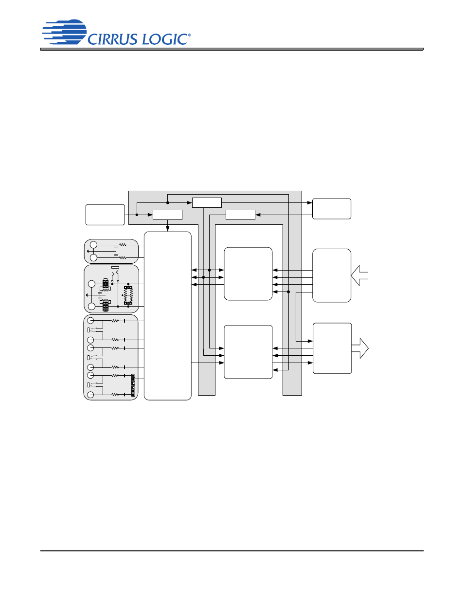
3. CONFIGURATION OPTIONS
This section shows two common configurations of the CDB42L56.
3.1
S/PDIF In to Analog Out and Analog In to S/PDIF Out
The CS42L56 ADC and DAC performance can be tested by loading the “SPDIF In to Analog Out -- Analog
In to S/PDIF Out” quick setup file provided with the software package. The script configures the digital clock
and data signal routing on the board as shown in
. The quick setup scripts provided in the software
assume that a 24.000 MHz on-board oscillator is populated in Y1.
A S/PDIF input must be provided as the S/PDIF Tx (CS8406) uses the RMCK signal from the S/PDIF Rx
(CS8416) for synchronization in this configuration, as shown in the
Line Output
B
A
HP Output
J21
32
32
16
16
J4
J12
B
A
AIN1A
AIN1B
AIN2A
AIN2B
AIN3A
AIN3B
J19
J20
LRCK
CS42L56
SCLK
SDIN
(SLAVE)
MCLK
SDOUT
LINEOUTB
LINEOUTA
HPOUTB
HPOUTA
AIN1A
AIN1B
AIN2A
AIN2B
AIN3A
AIN3B
S/PDIF Rx
(CS8416)
RX.LRCK
RX.SCLK
RX.SDOUT
S/PDIF
IN
(MASTER)
RX.RMCK
TX.SCLK
TX.LRCK
TX.SDIN
S/PDIF
OUT
(MASTER)
S/PDIF Tx
(CS8406)
TX.OMCK
FPGA
PLL
Divider
Divider
Divider
On-Board
Oscillator
Tx SRC
(CS8421)
(SLAVE)
ISCLK
ILRCK
SDIN
OSCLK
OLRCK
SDOUT
XTI
Rx SRC
(CS8421)
(SLAVE)
ISCLK
ILRCK
SDIN
OSCLK
OLRCK
SDOUT
XTI
Figure 2. S/PDIF In to Analog Out and Analog In to S/PDIF Out