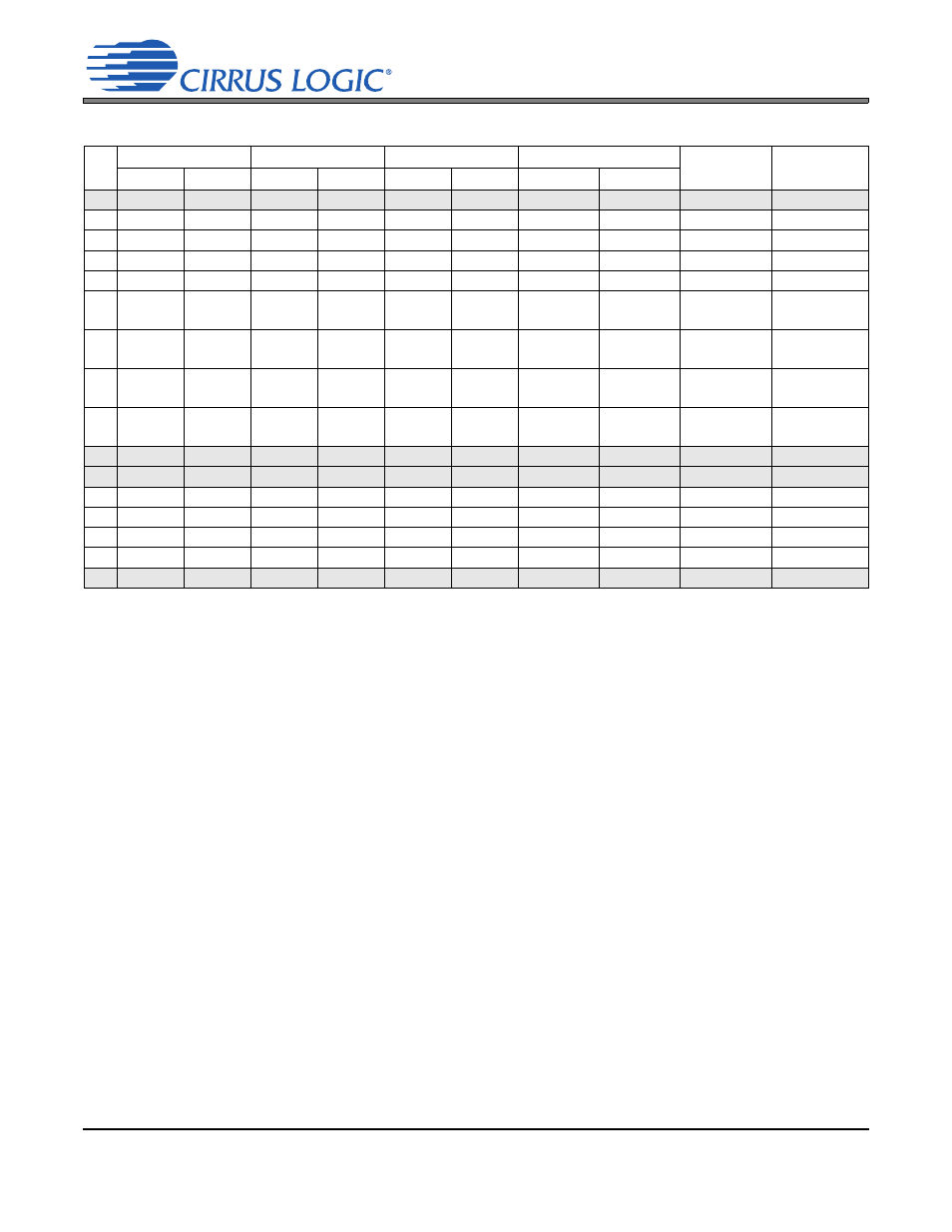
11 analog outputs, Table 1, Cdb42l56 – Cirrus Logic CDB42L56 User Manual
Page 7
DS851DB1
7
CDB42L56
Notes:
1. Use headers J7 and J11 to select input signal ground reference (in pseudo-differential mode) as either
the CDB42L56 board ground or the signal ground reference from the external system which the
CDB42L56 receives through the shield of the analog input cable.
2. Resistor modifications are only required if single-ended and pseudo-differential input configurations
need to be used simultaneously on the “A” and “B” inputs of the same analog input channel.
3. Resistor population settings for resistors not shown in the table should be the same as factory defaults.
illustrates how the analog inputs are connected and routed.
tails the jumper selections.
1.11 Analog Outputs
The CS42L56 analog outputs can be monitored on RCA jacks J15 and J17 for line and J37 and J38 for
headphone outputs. Additionally, the CS42L56 headphone outputs can also be monitored on stereo head-
phone jack J1 which also allows the user to test the CS42L56’s headphone detect functionality. The
CDB42L56 on-board circuitry drives the headphone detect pin low when a headphone is inserted in J1.
Headers J12 and J4 can be used to select optional 16
or 32 resistive loads for headphone outputs.
Headers J2 and J3 give users the option of receiving filtered or unfiltered outputs on the RCA headphone
output jacks.
illustrates how the analog outputs are connected and routed.
pro-
vides details on jumper selections for filtered or unfiltered outputs.
No. Analog Input 1
Analog Input 2
Analog Input 3
Jumper Settings
Resistors
to Populate
Resistors to
Unpopulate
AIN1A
AIN1B
AIN2A
AIN2B
AIN3A
AIN3B
J19
J20
1.
S.E.
S.E.
S.E.
S.E.
S.E.
S.E.
1-2
2-3
-
-
2.
S.E.
P.Diff.
S.E.
S.E.
-
S.E.
2-3
2-3
R86
R12
3.
P.Diff.
S.E.
S.E.
S.E.
-
S.E.
2-3
2-3
R41
R58
4.
S.E.
S.E.
S.E.
P.Diff.
S.E.
-
1-2
1-2
R109
R78
5.
S.E.
S.E.
P.Diff.
S.E.
S.E.
-
1-2
1-2
R51
R43
6.
S.E.
P.Diff.
P.Diff.
S.E.
-
-
2-3
1-2
R86
R51
R12
R43
7.
S.E.
P.Diff.
S.E.
P.Diff.
-
-
2-3
1-2
R86
R109
R12
R78
8.
P.Diff.
S.E.
S.E.
P.Diff.
-
-
2-3
1-2
R41
R109
R58
R78
9.
P.Diff.
S.E.
P.Diff.
S.E.
-
-
2-3
1-2
R41
R51
R58
R43
10.
S.E.
S.E.
P.Diff.
P.Diff.
S.E.
-
1-2
1-2
-
-
11.
P.Diff.
P.Diff.
S.E.
S.E.
-
S.E.
2-3
2-3
-
-
12.
S.E.
P.Diff.
P.Diff.
P.Diff.
-
-
2-3
1-2
R86
R12
13.
P.Diff.
S.E.
P.Diff.
P.Diff.
-
-
2-3
1-2
R41
R58
14.
P.Diff.
P.Diff.
S.E.
P.Diff.
-
-
2-3
1-2
R109
R78
15.
P.Diff.
P.Diff.
P.Diff.
S.E.
-
-
2-3
1-2
R51
R43
16.
P.Diff.
P.Diff.
P.Diff.
P.Diff.
-
-
2-3
1-2
-
-
Table 1. Analog Input Configuration Jumper and Resistor Settings