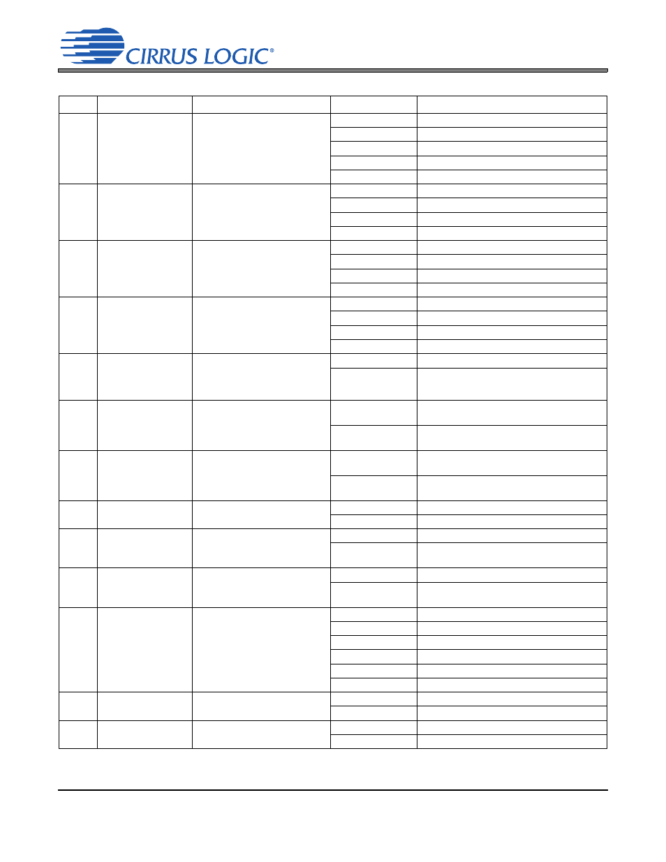
Table 3. jumper settings, Routed, Cdb42l56 – Cirrus Logic CDB42L56 User Manual
Page 19
19
DS851DB1
CDB42L56
JMP
LABEL
PURPOSE
POSITION
FUNCTION SELECTED
J31
VL
Selects source of voltage for the
VL supply
*+1.8V
Voltage source is +1.8 V regulator.
+2.5V
Voltage source is +2.5 V regulator.
+3.3V
Voltage source is +3.3 V regulator.
+1.8VB
Voltage source is +1.8 V from battery.
EXT. VL
Voltage source from TP18.
J36
VCP
Selects source of voltage for the
VCP supply
*+1.8V
Voltage source is +1.8 V regulator.
+2.5V
Voltage source is +2.5 V regulator.
+1.8VB
Voltage source is +1.8V from battery.
EXT. VCP
Voltage source from TP17.
J25
VA
Selects source of voltage for the
VA supply
*+1.8V
Voltage source is +1.8 V regulator.
+2.5V
Voltage source is +2.5 V regulator.
+1.8VB
Voltage source is +1.8 V from battery.
EXT. VA
Voltage source from TP5.
J28
VLDO
Selects source of voltage for the
VLDO supply
*+1.8V
Voltage source is +1.8 V regulator.
+2.5V
Voltage source is +2.5 V regulator.
+1.8VB
Voltage source is +1.8 V from battery.
EXT. VLDO
Voltage source from TP8.
J52
J74
J53
J48
VLDO
VA
VL
VCP
Current Measurement
*SHUNTED
1
series resistor is shorted.
OPEN
1
series resistor in power supply path.
J11
Shunt to RCA
Provides RCA reference to GND
*SHUNTED
AIN2REF and RCAs for AIN2A and AIN2B given
a board ground reference.
OPEN
AIN2REF is given AIN2A and AIN2B ground ref-
erence on RCA shield.
J7
Shunt to RCA
Provides RCA reference to GND
*SHUNTED
AIN1REF and RCAs for AIN1A and AIN1B given
a board ground reference.
OPEN
AIN1REF is given AIN1A and AIN1B ground ref-
erence on RCA shield.
J5
1.8 V Buck Input
Selects power supply source for
+1.8VB
1 - 2
1.8VB is derived from external input TP6.
*2 - 3
1.8VB is derived from AAA batteries.
J19
AIN3A/AIN1REF Input
Selects input source for pin
AIN3A/AIN1REF
*1 - 2
AIN3A/AIN1REF is given AIN3A input.
2 - 3
AIN3A/AIN1REF is given AIN1 ground reference
as input.
J20
AIN3B/AIN2REF Input
Selects input source for pin
AIN3B/AIN2REF
*1 - 2
AIN3B/AIN2REF is given AIN3B input.
2 - 3
AIN3B/AIN2REF is given AIN2 ground reference
as input.
J6
SHUNT TO APPLY
MICBIAS
Selects MICBIAS for analog inputs
1 - 3
MICBIAS applied to AIN1A.
2 - 4
MICBIAS applied to AIN1B.
5 - 6
MICBIAS applied to AIN2A.
7 - 8
MICBIAS applied to AIN2B.
9 - 10
MICBIAS applied to AIN3A.
11 - 12
MICBIAS applied to AIN3B.
J12
HPOUTA
Selects test load from HPOUTA
1 - 2
32
load selected for HPOUTA.
*2 - 3
16
load selected for HPOUTA.
J4
HPOUTB
Selects test load from HPOUTB
1 - 2
32
load selected for HPOUTB.
*2 - 3
16
load selected for HPOUTB.
Table 3. Jumper Settings
F
i
10