Cirrus Logic CDB42L56 User Manual
Cdb42l56, Evaluation board for cs42l56, Features
Copyright
Cirrus Logic, Inc. 2014
(All Rights Reserved)
Evaluation Board for CS42L56
Features
Analog Line and Microphone Level Inputs
–
6 RCA and 3 Stereo 1/8” Jacks
–
Compatible with Single-Ended and Pseudo-Diff.
Input Configurations
Analog Line and Headphone Outputs
–
Stereo 1/8” Headphone Jack w/Input Detection
–
4 RCA Jacks for Headphone/Line Outputs
8 to 96 kHz S/PDIF Interface
–
CS8416 Digital Audio Receiver
–
CS8406 Digital Audio Transmitter
I/O Stake Header Accessibility
–
External Control Port Headers
–
External Direct and Buffered Serial Audio I/O
Headers
Multiple Power Supply options via USB, Battery or
External Power Supplies.
1.8 V to 3.3 V Selectable Logic Interface
FlexGUI S/W Control - Windows
®
Compatible
–
Pre-Defined & User-Configurable Scripts
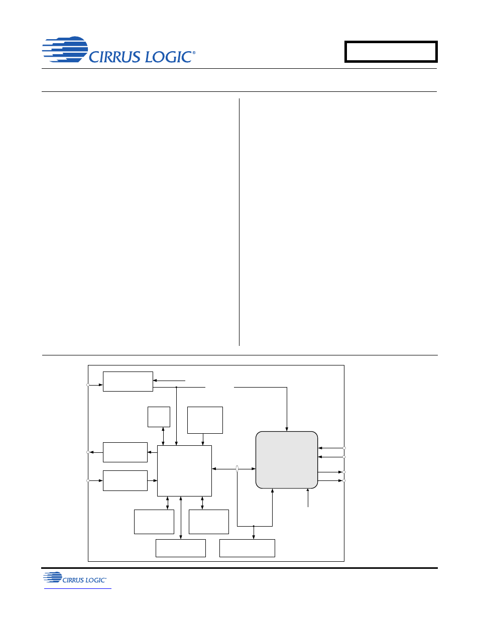
Description
The CDB42L56 is the ideal evaluation platform solution to test
and evaluate the CS42L56.The CS42L56 is a highly integrat-
ed, 24-bit, ultra-low power stereo codec based on multi-bit
delta-sigma modulation suitable for low power portable appli-
cations. Use of the board requires an analog/digital signal
source, an analyzer and power supplies. A Windows PC-com-
patible computer is also needed in order to configure the
CS42L56 and the board.
System timing can be provided by the CS8416 (on-board), by
the CS42L56 supplied with a master clock, by the on-board
crystal oscillator or via an I/O stake header with a DSP
connected.
RCA phono connectors and stereo 1/8
th
inch audio jacks are
provided for CS42L56 analog inputs and HP/Line outputs.
Digital I/O connections are provided via RCA phono or optical
connectors to the CS8416 and CS8406 (S/PDIF Rx and Tx).
The CDB42L56 is programmed via the PC’s USB using Cirrus
Logic’s Microsoft
®
Windows
®
-based software (FlexGUI). The
evaluation board may also be configured to accept external
timing and data signals for operation in a user application
during system development.
ORDERING INFORMATION
CDB42L56 Evaluation Board
USB
µ controller
CS42L56
S/PDIF Rx
(CS8416)
S/PDIF Tx
(CS8406)
FPGA
Oscillator
(socket)
I
2
C Interface
Reset
Reset
PLL
Tx SRC
(CS8421)
Analog Outputs
(Line + Headphone)
Analog Inputs
(Line + MIC)
External System
I/O Header
Rx SRC
(CS8421)
PSIA I/O Header
USB/
RS232
S/PDIF
Dout
S/PDIF
Din
FEB '14
DS851DB1
CDB42L56
Document Outline
- 1. SYSTEM OVERVIEW
- 2. QUICK-START GUIDE
- 3. Configuration Options
- 4. Software Mode Control
- 5. Jumper Settings and System Connections
- 6. Performance Plots
- Figure 10. THD+N vs. Freq. - Analog In to Digital Out
- Figure 11. THD+N vs. Amplitude - Analog In to Digital Out
- Figure 12. FFT - Analog In to Digital Out @ -1 dBFS
- Figure 13. FFT - Analog In to Digital Out @ -60 dBFS
- Figure 14. FFT - Analog In to Digital Out - No Input
- Figure 15. FFT Crosstalk - Analog In to Digital Out @ -1 dBFS
- Figure 16. Freq. Response - Analog In to Digital Out
- Figure 17. Fade-to-Noise Linearity - Analog In to Digital Out
- Figure 18. THD+N vs. Freq. - Digital In to HP Out
- Figure 19. THD+N vs. Amplitude - Digital In to HP Out
- Figure 20. FFT - Digital In to HP Out @ -60 dBFS
- Figure 21. FFT - Digital In to HP Out - No Input
- Figure 22. FFT - Digital In to HP Out - No Input Wideband
- Figure 23. FFT Crosstalk - Digital In to HP Out @ 0 dBFS
- Figure 24. Freq. Response - Digital In to HP Out
- Figure 25. Fade-to-Noise Linearity- Digital In to HP Out
- Figure 26. THD+N vs. Freq. - Digital In to Line Out
- Figure 27. THD+N vs. Amplitude - Digital In to Line Out
- Figure 28. FFT - Digital In to Line Out @ 0 dBFS
- Figure 29. FFT - Digital In to Line Out @ -60 dBFS
- Figure 30. FFT - Digital In to Line Out - No Input
- Figure 31. FFT - Digital In to Line Out - No Input Wideband
- Figure 32. Freq. Response - Digital In to Line Out
- Figure 33. Fade-to-Noise Linearity- Digital In to Line Out
- 7. CDB42L56 Block Diagram
- 8. CDB42L56 Schematics
- 9. CDB42L56 Layout
- 10. Revision History