Cirrus Logic CDB4265 User Manual
Features, Description
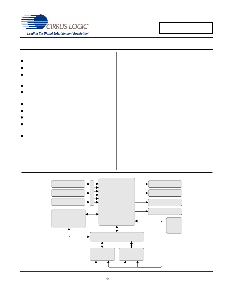
Table of contents
Document Outline
- Features
- Description
- Table of Contents
- List of Figures
- List of Tables
- 1. System Overview
- 2. System Clocks and Data
- 3. PC Software Control
- 4. FPGA Register Quick Reference
- 5. FPGA Register Description
- 5.1 Code Revision ID - Register 01h
- 5.2 MCLK Source Control - Address 02h
- Table 1. MCLK Source
- 5.3 Subclock Source Control - Address 03h
- Table 2. CS4265 Subclock Source
- 5.4 CS4265 SDIN Source Control - Address 04h
- Table 3. SDIN2 Source
- Table 4. SDIN1 Source
- 5.5 Transmitter SDIN Source Control - Address 05h
- Table 5. TXSDIN Source
- 6. CDB Connectors, Jumpers, and Switches
- 7. CDB Block Diagram
- 8. CDB Schematics
- 9. CDB Layout
- 10. Revision History