Cirrus Logic CDB4265 User Manual
Features, Description
Copyright
© Cirrus Logic, Inc. 2005
(All Rights Reserved)
Cirrus Logic, Inc.
www.cirrus.com
CDB4265
Evaluation Board for CS4265
Features
z
Single-ended Analog Inputs
z
Single-ended Analog Outputs
z
Coaxial and Optical Connections for CS4265
S/PDIF Transmitter Output
z
CS8416 S/PDIF Digital Audio Receiver
z
Header for Optional External Software
Configuration of CS4265
z
Header for External PCM Serial Audio I/O
z
3.3 V Logic Interface
z
Pre-defined Software Scripts
z
Demonstrates Recommended Layout and
Grounding Arrangements
z
Windows
®
Compatible Software Interface
to Configure CS4265 and Inter-board
Connections
ORDERING INFORMATION
CDB4265
Evaluation Board
Description
The CDB4265 evaluation board is an excellent means
for evaluating the CS4265 CODEC. Evaluation requires
an analog/digital signal source and analyzer, and power
supplies. A Windows
®
PC compatible computer must be
used to evaluate the CS4265.
System timing for the I²S, Left-Justified and Right-Justi-
fied interface formats can be provided by the CS4265,
the CS8416, or by a PCM I/O stake header with an ex-
ternal source connected.
RCA phono jacks are provided for the CS4265 analog in-
puts and outputs. Digital data I/O is available via RCA
phono or optical connectors to the CS8416 and CS4265.
The Windows
®
software provides a GUI to make config-
uration of the CDB4265 easy. The software
communicates through the PC’s serial port to configure
the control port registers so that all features of the
CS4265 can be evaluated. The evaluation board may
also be configured to accept external timing and data
signals for operation in a user application during system
development.
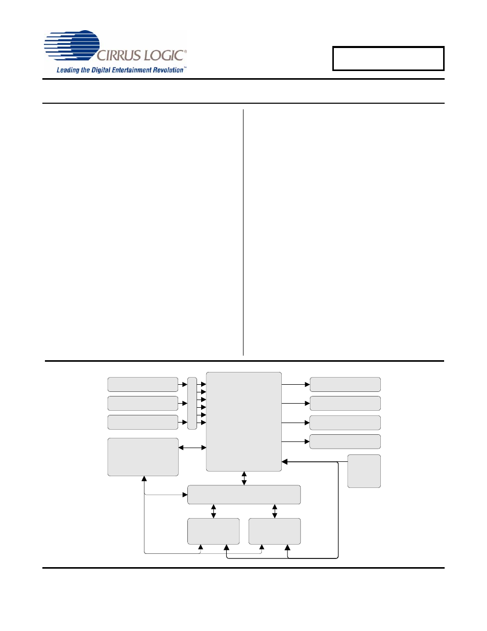
I
CS4265
Passive Input Filter
Active Input Filter
Header
Microphone Input
S/PDIF Output Circuits
Canned
Oscillator
Control Port Interface
Test Points
M
U
X
Master Clock
Passive Output Filter
Active Output Filter
CS8416
FPGA
Sub-clocks and Data
FEB ‘05
DS657DB1
Document Outline
- Features
- Description
- Table of Contents
- List of Figures
- List of Tables
- 1. System Overview
- 2. System Clocks and Data
- 3. PC Software Control
- 4. FPGA Register Quick Reference
- 5. FPGA Register Description
- 5.1 Code Revision ID - Register 01h
- 5.2 MCLK Source Control - Address 02h
- Table 1. MCLK Source
- 5.3 Subclock Source Control - Address 03h
- Table 2. CS4265 Subclock Source
- 5.4 CS4265 SDIN Source Control - Address 04h
- Table 3. SDIN2 Source
- Table 4. SDIN1 Source
- 5.5 Transmitter SDIN Source Control - Address 05h
- Table 5. TXSDIN Source
- 6. CDB Connectors, Jumpers, and Switches
- 7. CDB Block Diagram
- 8. CDB Schematics
- 9. CDB Layout
- 10. Revision History