Figure 14. de-emphasis curve, 5 analog connections, 1 input component values – Cirrus Logic CS4270 User Manual
Page 25: Table 8. analog input design parameters, Figure 14, Cs4270
DS686F1
25
CS4270
5.5
Analog Connections
The analog modulator samples the input at 6.144 MHz for Fs = 48, 96, and 128 kHz and scales propor-
tionally for all other sampling speeds.The digital filter rejects signals within the stopband of the filter. How-
ever, there is no rejection for input signals that are multiples of the input sampling frequency (e.g.,
n
6.144 MHz), where n = 0, 1, 2, ... .
shows the recommended topology of the analog input
network. The capacitor values are chosen not only provide the appropriate filtering of noise at the modu-
lator sampling frequency, but to act as a charge source for the internal sampling circuits. The use of ca-
pacitors with a large voltage coefficient (such as general-purpose ceramics) can degrade signal linearity.
5.5.1
Input Component Values
shows the three parameters (source impedance, attenuation, and input impedance) that deter-
mine the values of resistors R1 and R2, as seen in
, and shows the design equations used to
determine these values.
illustrates an example configuration using two 2-k
resistors in place of R1 and R2. This circuit
will attenuate a typical line level voltage, 2 Vrms, to the full-scale input of the ADC,
(1 Vrms) when
VA = 5 V.
Parameter
Equation
Source Impedance: The impedance as seen from the ADC looking back into the signal
network. The ADC achieves optimal THD+N performance when source impedance less
than or equal to 1.0 k
and
.
Attenuation: The required attenuation factor depends on the magnitude of the input sig-
nal. For VA = 5 V, the full-scale input voltage equals
(1 Vrms). See
on page 11. The user should select values for R1 and R2 such that the
magnitude of the incoming signal multiplied by the attenuation factor is less than or equal
to the full-scale input voltage of the device.
Input Impedance: Input impedance is the impedance from the signal source to the ADC
analog input pins.
shows the input parameters and the associated design equa-
tions.
Table 8. Analog Input Design Parameters
Gain
dB
-10dB
0dB
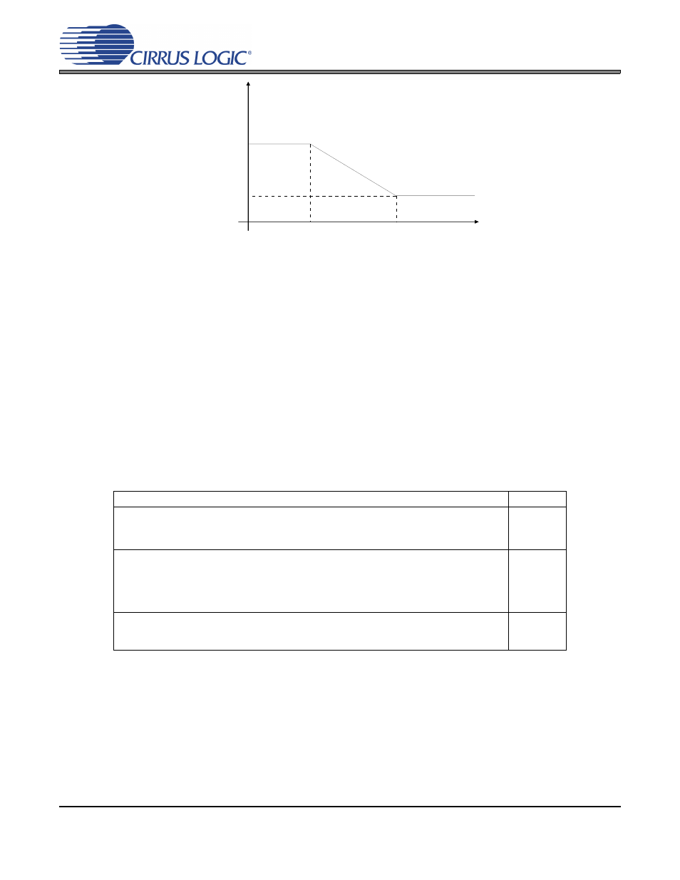
Frequency
T2 = 15 µs
T1=50 µs
F1
F2
3.183 kHz
10.61 kHz
Figure 14. De-Emphasis Curve
R1 R2
R1 R2
+
-------------------------
R2
R1 R2
+
-------------------------
R1 R2
+