4 analog input multiplexer, pga, and mic gain, Figure 11. analog input architecture, 5 input connections – Cirrus Logic CS4265 User Manual
Page 27: 1 pseudo-differential input, Figure 11.analog input architecture, Cs4265
DS657F3
27
CS4265
4.4
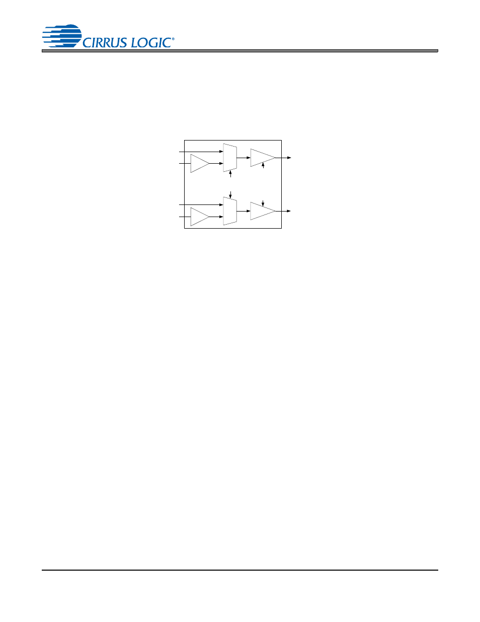
Analog Input Multiplexer, PGA, and Mic Gain
The CS4265 contains a stereo 2-to-1 analog input multiplexer followed by a programmable gain amplifier
(PGA). The input multiplexer is able to select either a line-level input source, or a mic-level input source, and
route it to the PGA. The mic-level input passes through a +32 dB gain stage prior to the input multiplexer,
allowing it to be used for microphone-level signals without the need for any external gain. The PGA stage
provides 12 dB of gain or attenuation in 0.5 dB steps.
shows the architecture of the input multi-
plexer, PGA, and mic gain stages.
The
“Analog Input Selection (Bit 0)” on page 41
outlines the bit settings necessary to control the input mul-
tiplexer and mic gain.
“Channel B PGA Control - Address 07h” on page 40
outline the register settings necessary to control the PGA. By default, the line-
level input is selected by the input multiplexer, and the PGA is set to 0 dB.
4.5
Input Connections
The analog modulator samples the input at 6.144 MHz (MCLK=12.288 MHz). The digital filter will reject sig-
nals within the stopband of the filter. However, there is no rejection for input signals
which are
(n
6.144 MHz) the digital passband frequency, where n=0,1,2,... Refer to the Typical Connection Diagram
for the recommended analog input circuit that will attenuate noise energy at 6.144 MHz. The use of capac-
itors which have a lar ge voltage coefficient (such as ge neral-purpose ceramics) must be avoided since
these can degrade signal linearity. Any unused analog input pairs should be left unconnected.
4.5.1
Pseudo-Differential Input
The CS4265 implements a pseudo-differential input stage. The SGND input is intended to be used as a
pseudo-differential reference signal. This feature allows for common mode noise rejection with single-
ended signals.
shows a basic diagram outlining the internal implementation of the pseudo-dif-
ferential input stage. The Typical Connection Diagram shows the recommended pseudo-differential input
PGA
MUX
+32 dB
AINA
MICIN1
Channel B
PGA Gain Bits
Out to ADC
Channel A
Out to ADC
Channel B
MUX
+32 dB
AINB
MICIN2
PGA
Analog Input
Selection Bits
Channel A
PGA Gain Bits
Figure 11. Analog Input Architecture