Cirrus Logic CS4265 User Manual
Cs4265, D/a features, A/d features
Copyright
Cirrus Logic, Inc. 2012
(All Rights Reserved)
104 dB, 24-Bit, 192 kHz Stereo Audio CODEC
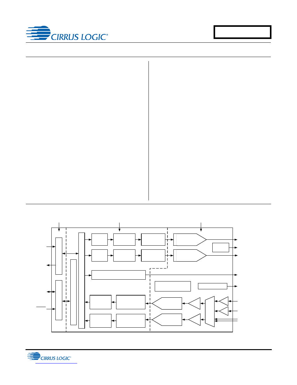
D/A Features
Multi-Bit Delta Sigma Modulator
104 dB Dynamic Range
-90 dB THD+N
Up to 192 kHz Sampling Rates
Single-Ended Analog Architecture
Volume Control with Soft Ramp
– 0.5 dB Step Size
– Zero Crossing, Click-Free Transitions
Popguard
®
Technology
– Minimizes the Effects of Output Transients
Filtered Line-Level Outputs
Selectable Serial Audio Interface Formats
– Left-Justified up to 24-bit
– I²S up to 24-bit
– Right-Justified 16-, 18-, 20-, and 24-bit
Selectable 50/15 µs De-Emphasis
A/D Features
Multi-Bit Delta Sigma Modulator
104 dB Dynamic Range
-95 dB THD+N
Stereo 2:1 Input Multiplexer
Programmable Gain Amplifier (PGA)
– ± 12 dB Gain, 0.5 dB Step Size
– Zero Crossing, Click-Free Transitions
Pseudo-Differential Stereo Line Inputs
Stereo Microphone Inputs
– +32 dB Gain Stage
– Low-Noise Bias Supply
Up to 192 kHz Sampling Rates
Selectable Serial Audio Interface Formats
– Left-Justified up to 24-bit
– I²S up to 24-bit
High-Pass Filter or DC Offset Calibration
1.8 V to 5 V
Multibit
Modulator
Multibit
Modulator
Low-Latency
Anti-Alias Filter
Interpolation
Filter
Interpolation
Filter
Left DAC Output
Right DAC Output
Switched Capacitor
DAC and Filter
Multibit
Oversampling
ADC
Multibit
Oversampling
ADC
Low-Latency
Anti-Alias Filter
High Pass
Filter
High Pass
Filter
Stereo
Line Input
Serial
Audio
Input
Serial
Audio
Output
3.3 V to 5 V
3.3 V to 5 V
Switched Capacitor
DAC and Filter
MUX
PGA
Volume
Control
Volume
Control
PC
M
Ser
ial
Int
er
fa
ce
/ L
oop
bac
k
Mute
Control
Le
vel
Tra
nslat
or
Le
vel
Tr
an
sl
at
or
Reset
I
2
C Control
Data
Mute Control
Mic Input
1 & 2
PGA
+32 dB
+32 dB
Internal Voltage
Reference
IEC60958-3 Transmitter
Mic Bias
Microphone Bias
Transmitter Output
R
egist
er
Conf
igur
at
io
n
AUG '12
DS657F3
CS4265
Document Outline
- 1. Pin Descriptions
- 2. Characteristics and Specifications
- Specified Operating Conditions
- Absolute Maximum Ratings
- DAC Analog Characteristics
- DAC Combined Interpolation & On-Chip Analog FIlter Response
- ADC Analog Characteristics
- ADC Analog Characteristics
- ADC Digital Filter Characteristics
- DC Electrical Characteristics
- Digital Interface Characteristics
- Switching Characteristics - Serial Audio Port
- Switching Characteristics - I·C Control Port
- 3. Typical Connection Diagram
- 4. Applications
- 4.1 Recommended Power-Up Sequence
- 4.2 System Clocking
- 4.3 High-Pass Filter and DC Offset Calibration
- 4.4 Analog Input Multiplexer, PGA, and Mic Gain
- 4.5 Input Connections
- 4.6 Output Connections
- 4.7 Output Transient Control
- 4.8 DAC Serial Data Input Multiplexer
- 4.9 De-Emphasis Filter
- 4.10 Internal Digital Loopback
- 4.11 Mute Control
- 4.12 AES3 Transmitter
- 4.13 I·C Control Port Description and Timing
- 4.14 Status Reporting
- 4.15 Reset
- 4.16 Synchronization of Multiple Devices
- 4.17 Grounding and Power Supply Decoupling
- 4.18 Package Considerations
- 5. Register Quick Reference
- 6. Register Description
- 6.1 Chip ID - Register 01h
- 6.2 Power Control - Address 02h
- 6.3 DAC Control - Address 03h
- 6.4 ADC Control - Address 04h
- 6.5 MCLK Frequency - Address 05h
- 6.6 Signal Selection - Address 06h
- 6.7 Channel B PGA Control - Address 07h
- 6.8 Channel A PGA Control - Address 08h
- 6.9 ADC Input Control - Address 09h
- 6.10 DAC Channel A Volume Control - Address 0Ah
- 6.11 DAC Channel B Volume Control - Address 0Bh
- 6.12 DAC Control 2 - Address 0Ch
- 6.13 Status - Address 0Dh
- 6.14 Status Mask - Address 0Eh
- 6.15 Status Mode MSB - Address 0Fh
- 6.16 Status Mode LSB - Address 10h
- 6.17 Transmitter Control 1 - Address 11h
- 6.18 Transmitter Control 2 - Address 12h
- 6.18.1 Transmitter Digital Interface Format (Bits 7:6)
- 6.18.2 Transmitter Output Driver Control (Bit 5)
- 6.18.3 Transmitter Mute Control (Bit 4)
- 6.18.4 Transmitted Validity Bit Control (Bit 3)
- 6.18.5 Transmitter Mono/Stereo Operation Control (Bit 2)
- 6.18.6 Mono Mode CS Data Source (Bit 1)
- 6.18.7 Mono Mode Channel Selection (Bit 0)
- 7. Parameter Definitions
- 8. DAC Filter Plots
- Figure 18. DAC Single-Speed Stopband Rejection
- Figure 19. DAC Single-Speed Transition Band
- Figure 20. DAC Single-Speed Transition Band
- Figure 21. DAC Single-Speed Passband Ripple
- Figure 22. DAC Double-Speed Stopband Rejection
- Figure 23. DAC Double-Speed Transition Band
- Figure 24. DAC Double-Speed Transition Band
- Figure 25. DAC Double-Speed Passband Ripple
- Figure 26. DAC Quad-Speed Stopband Rejection
- Figure 27. DAC Quad-Speed Transition Band
- Figure 28. DAC Quad-Speed Transition Band
- Figure 29. DAC Quad-Speed Passband Ripple
- 9. ADC Filter Plots
- Figure 30. ADC Single-Speed Stopband Rejection
- Figure 31. ADC Single-Speed Stopband Rejection
- Figure 32. ADC Single-Speed Transition Band (Detail)
- Figure 33. ADC Single-Speed Passband Ripple
- Figure 34. ADC Double-Speed Stopband Rejection
- Figure 35. ADC Double-Speed Stopband Rejection
- Figure 36. ADC Double-Speed Transition Band (Detail)
- Figure 37. ADC Double-Speed Passband Ripple
- Figure 38. ADC Quad-Speed Stopband Rejection
- Figure 39. ADC Quad-Speed Stopband Rejection
- Figure 40. ADC Quad-Speed Transition Band (Detail)
- Figure 41. ADC Quad-Speed Passband Ripple
- 10. External IEC60958-3 Transmitter Components
- 11. Channel Status Buffer Management
- 12. Package Dimensions
- 13. Thermal Characteristics and Specifications
- 14. Ordering Information
- 15. Revision History