Block diagram – Analog Devices ADSP-21020 User Manual
Page 3
ADSP-21020
REV. C
–3–
the standard IEEE format, whereas the 40-bit IEEE extended-
precision format has eight additional LSBs of mantissa for
greater accuracy.
The multiplier performs floating-point and fixed-point
multiplication as well as fixed-point multiply/add and multiply/
subtract operations. Integer products are 64 bits wide, and the
accumulator is 80 bits wide. The ALU performs 45 standard
arithmetic and logic operations, supporting both fixed-point and
floating-point formats. The shifter performs 19 different
operations on 32-bit operands. These operations include logical
and arithmetic shifts, bit manipulation, field deposit, and extract
and derive exponent operations.
The computation units perform single-cycle operations; there is
no computation pipeline. The three units are connected in
parallel rather than serially, via multiple-bus connections with
the 10-port data register file. The output of any computation
unit may be used as the input of any unit on the next cycle. In a
multifunction computation, the ALU and multiplier perform
independent, simultaneous operations.
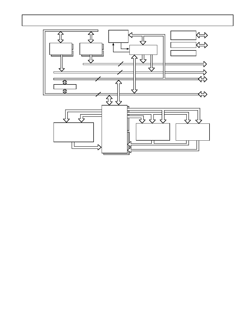
Data Register File
The ADSP-21020’s general-purpose data register file is used for
transferring data between the computation units and the data
buses, and for storing intermediate results. The register file has
two sets (primary and alternate) of sixteen 40-bit registers each,
for fast context switching.
With a large number of buses connecting the registers to the
computation units, data flow between computation units and
from/to off-chip memory is unconstrained and free from
bottlenecks. The 10-port register file and Harvard architecture
of the ADSP-21020 allow the following nine data transfers to be
performed every cycle:
•
Off-chip read/write of two operands to or from the register file
•
Two operands supplied to the ALU
•
Two operands supplied to the multiplier
•
Two results received from the ALU and multiplier (three, if
the ALU operation is a combined addition/subtraction)
The processor’s 48-bit orthogonal instruction word supports
fully parallel data transfer and arithmetic operations in the same
instruction.
Address Generators and Program Sequencer
Two dedicated address generators and a program sequencer
supply addresses for memory accesses. Because of this, the
computation units need never be used to calculate addresses.
Because of its instruction cache, the ADSP-21020 can
simultaneously fetch an instruction and data values from both
off-chip program memory and off-chip data memory in a single
cycle.
The data address generators (DAGs) provide memory addresses
when external memory data is transferred over the parallel
memory ports to or from internal registers. Dual data address
generators enable the processor to output two simultaneous
addresses for dual operand reads and writes. DAG 1 supplies
32-bit addresses to data memory. DAG 2 supplies 24-bit
addresses to program memory for program memory data
accesses.
Each DAG keeps track of up to eight address pointers, eight
modifiers, eight buffer length values and eight base values. A
pointer used for indirect addressing can be modified by a value
DAG 2
8 x 4 x 24
DAG 1
8 x 4 x 32
CACHE
MEMORY
32 x 48
PROGRAM
SEQUENCER
PMD BUS
DMD BUS
24
PMA BUS
PMD
DMD
PMA
32
DMA BUS
DMA
48
40
JTAG TEST &
EMULATION
FLAGS
FLOATING & FIXED-POINT
MULTIPLIER, FIXED-POINT
ACCUMULATOR
32-BIT
BARREL
SHIFTER
FLOATING-POINT
& FIXED-POINT
ALU
REGISTER
FILE
16 x 40
BUS CONNECT
TIMER
Figure 1. ADSP-21020 Block Diagram