Ampro Corporation CoreModule 420 5001692A User Manual
Page 30
Chapter 3
Hardware
24
Reference Manual
CoreModule 420
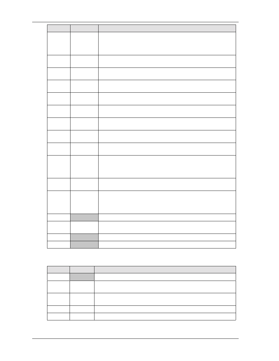
Pin #
Signal
Description (P1 Row B)
49 (B17)
DAck1*
DMA Acknowledge 1 – Used by DMA controller to select the I/O
resource requesting the bus, or to request ownership of the bus as a bus
master device. Can also be used by the ISA bus master to gain control
of the bus from the DMA controller.
50 (B18)
DRQ1
DMA Request 1 – Used by I/O resources to request DMA service.
Must be held high until associated DACK1 line is active.
51 (B19)
Refresh*
Memory Refresh – This signal is driven low to indicate a memory
refresh cycle is in progress. Memory is refreshed every 15.6 usec.
52 (B20)
SysClk*
System Clock – This is a free running clock typically in the 8MHZ to
10MHz range, although its exact frequency is not guaranteed.
53 (B21)
IRQ7
Interrupt Request 7 – Asserted by a device when it has pending interrupt
request. Only one device may use the request line at a time.
54 (B22)
IRQ6
Interrupt Request 6 – Asserted by a device when it has pending interrupt
request. Only one device may use the request line at a time.
55 (B23)
IRQ5
Interrupt Request 5 – Asserted by a device when it has pending interrupt
request. Only one device may use the request line at a time.
56 (B24)
IRQ4
Interrupt Request 4 – Asserted by a device when it has pending interrupt
request. Only one device may use the request line at a time.
57 (B25)
IRQ3
Interrupt Request 3 – Asserted by a device when it has pending interrupt
request. Only one device may use the request line at a time.
58 (B26)
DAck2*
DMA Acknowledge 2 – Used by DMA controller to select the I/O
resource requesting the bus, or to request ownership of the bus as a bus
master device. Can also be used by the ISA bus master to gain control
of the bus from the DMA controller.
59 (B27)
TC
Terminal Count – This signal is a pulse to indicate a terminal count has
been reached on a DMA channel operation.
60 (B28)
BALE
Buffered Address Latch Enable – This signal is used to latch the LA23
to LA17 signals or decodes of these signals. Addresses are latched on
the falling edge of BALE. It is forced high during DMA cycles. When
used with AENx, it indicates a valid processor or DMA address.
61 (B29)
+5V
+5V power +/- 10%
62 (B30)
OSC
Oscillator – This clock signal operates at 14.3MHz. This signal is not
synchronous with the system clock (SYSCLK).
63 (B31)
GND
Ground
64 (B32)
GND
Ground
Notes: The shaded area denotes power or ground. The signals marked with * indicate active low.
Table 3-7. PC/104 Bus Interface Pin/Signal Descriptions (P1C)
Pin #
Signal
Description (P1 Row C)
1 (C0)
GND
Ground
2 (C1)
SBHE*
System Byte High Enable – This signal is driven low to indicate a transfer
of data on the high half of the data bus (D15 to D8).
3 (C2)
LA23
Lactchable Address 23 – This signal must be latched by the resource if the
line is required for the entire data cycle.
4 (C3)
LA22
Lactchable Address 22 – Refer to LA23, pin C2, for more information.
5 (C4)
LA21
Lactchable Address 21 – Refer to LA23, pin C2, for more information.