Pc/104 bus interface (p1a,b,c,d) – Ampro Corporation CoreModule 420 5001692A User Manual
Page 28
Chapter 3
Hardware
22
Reference Manual
CoreModule 420
PC/104 Bus Interface (P1A,B,C,D)
The PC/104 Bus uses a 104-pin 0.1” connector interface. This interface connector will carry all of the
appropriate PC/104 signals operating at clock speeds up to 8.25MHz. This interface connector is located
on the both the top and bottom of the module.
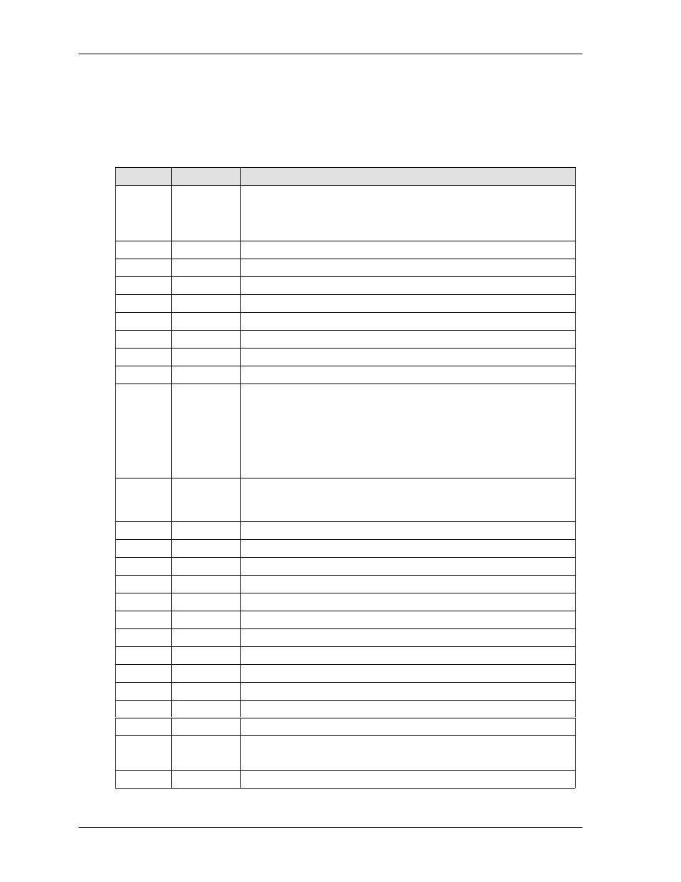
Table 3-5. PC/104 Bus Interface Pin/Signal Descriptions (P1A)
Pin #
Signal
Description (P1 Row A)
1 (A1)
IOCHCHK*
I/O Channel Check – This signal may be activated by ISA boards to
request that a non-maskable interrupt (NMI) be generated to the system
processor. It is driven active to indicate an uncorrectable error has been
detected.
2 (A2)
SD7
System Data 7 – This signal (0 to 19) provides a system data bit.
3 (A3)
SD6
System Data 6 – Refer to SD7, pin A2, for more information.
4 (A4)
SD5
System Data 5 – Refer to SD7, pin A2, for more information.
5 (A5)
SD4
System Data 4 – Refer to SD7, pin A2, for more information.
6 (A6)
SD3
System Data 3 – Refer to SD7, pin A2, for more information.
7 (A7)
SD2
System Data 2 – Refer to SD7, pin A2, for more information.
8 (A8)
SD1
System Data 1 – Refer to SD7, pin A2, for more information.
9 (A9)
SD0
System Data 0 – Refer to SD7, pin A2, for more information.
10 (A10)
IOCHRDY
I/O Channel Ready – This signal allows slower ISA boards to lengthen
I/O or memory cycles by inserting wait states. This signal’s normal
state is active high (ready). ISA boards drive the signal inactive low
(not ready) to insert wait states. Devices using this signal to insert wait
states should drive it low immediately after detecting a valid address
decode and an active read, or write command. The signal is released
high when the device is ready to complete the cycle.
11 (A11)
AEn
Address Enable – This signal is reserved for the ISA Bus and is asserted
during DMA cycles to prevent I/O slaves from misinterpreting DMA
cycles as valid I/O cycles..
12 (A12)
SA19
System Address 19 – This signal (0 to 19) provides a system address bit.
13 (A13)
SA18
System Address 18 – Refer to SA19, pin A12, for more information.
14 (A14)
SA17
System Address 17 – Refer to SA19, pin A12, for more information.
15 (A15)
SA16
System Address 16 – Refer to SA19, pin A12, for more information.
16 (A16)
SA15
System Address 15 – Refer to SA19, pin A12, for more information.
17 (A17)
SA14
System Address 14 – Refer to SA19, pin A12, for more information.
18 (A18)
SA13
System Address 13 – Refer to SA19, pin A12, for more information.
19 (A19)
SA12
System Address 12– Refer to SA19, pin A12, for more information.
20 (A20)
SA11
System Address 11 – Refer to SA19, pin A12, for more information.
21 (A21)
SA10
System Address 10 – Refer to SA19, pin A12, for more information.
22 (A22)
SA9
System Address 9 – Refer to SA19, pin A12, for more information.
23 (A23)
SA8
System Address 8 – Refer to SA19, pin A12, for more information.
24 (A24)
SA7
System Address 7 – Refer to SA19, pin A12, for more information.
25 (A25)
SA6
System Address 6 – Refer to SA19, pin A12, for more information.
26 (A26)
SA5
System Address 5 – Refer to SA19, pin A12, for more information.