C requirements, C register write, Table 4-2: spi timing specifications – PNI RM3100 Evaluation Board User Manual
Page 15: Symbol description min max units, A generic write transaction is given below

PNI Sensor Corporation
Doc 1017252 r02
RM3100 Evaluation Board User Manual
Page 14 of 33
Table 4-2: SPI Timing Specifications
Symbol
Description
Min
Max
Units
t
SHZD
SSN LOW to data output
100
ns
t
SSDV
SSN LOW to Command Byte
100
ns
t
DBSH
Setup data before active edge
50
ns
t
DASH
Hold data after active edge
50
ns
t
DRDV
Clock falling edge to valid data
10
ns
t
SSH
Final clock cycle falling edge to SSN HIGH
100
ns
t
SHDZ
SSN HIGH to output data tri-state
100
ns
t
SSW
SSN HIGH to LOW (time between transactions)
100
4.5 I
2
C Requirements
The RM3100 Eval Board can operate as a slave device on either an I
2
C or SPI bus. This
section discusses basic requirements for operation on an I
2
C bus. The module is identified by
a 7-bit slave address, where the higher 5 bits of the slave address are pre-defined in hardware
and the same for all RM3100 Evaluation Boards. PNI has registered these first 5 bits as
0b01000. The lower 2 bits of the slave address are user-configurable, using pins 3 and 28.
As such, 4 different slave addresses are possible. For example, setting pin 3 HIGH and pin
28 LOW results in an address of 0b0100001.
The RM3100 Evaluation Board’s I
2
C interface complies with NXP’s UM10204 specification
and user manual, revision 03. Standard, fast, fast plus, and high speed modes of the I
2
C
protocol are supported. Below is a link to this document.
4.5.1 I
2
C Register Write
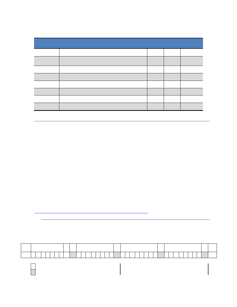
A generic Write transaction is given below.
START
RM3100 Eval Board
ADDRESS
RW ACK
RM3100 Eval Board
REG. ADDRESS (N)
ACK
DATA TO REGISTER (N)
ACK DATA TO REGISTER (N+1) ACK STOP
S
A6 A5 A4 A3 A2 A1 A0 0
0 A7 A6 A5 A4 A3 A2 A1 A0 0 A7 A6 A5 A4 A3 A2 A1 A0 0 A7 A6 A5 A4 A3 A2 A1 A0 0
P
From Host to RM3100 E.B.
------------ Data Transferred (n bytes + acknowledge) ------------
From RM3100 E.B. to Host
