PNI ASIC User Manual
Pni asic, General description, Features
PNI ASIC
3-Axis Magneto-Inductive Sensor Driver and Controller
with SPI Serial Interface
General Description
The PNI (11096) ASIC is a low cost magnetic
Measurement Application Specific Integrated Circuit
designed for use with PNI Corporation’s magneto-
inductive sensors. The PNI ASIC can control and
measure three independent magneto-inductive
sensors. Each sensor is individually selectable for
measurement, and can also be individually
configured for measurement resolution. The PNI
ASIC has diagnostic modes and outputs to test the
oscillator and counter circuits.
The PNI ASIC contains the entire measurement
circuit, both analog and digital sections. Each sensor
changes its inductance with an applied change in
magnetic field parallel to the sensor. In order to make
a measurement, the sensor is switched into an L/R
oscillator circuit. The bipolar differential
measurement scheme used by the PNI ASIC makes
the magnetic measurement inherently temperature
independent. It also has the benefit of transforming
the measurement range into a zero centered, positive/
negative value.
Features
Low supply current:
<500 µA at 3 VDC
<1 µA, idle mode
Complete 3-axis magnetic sensor driver
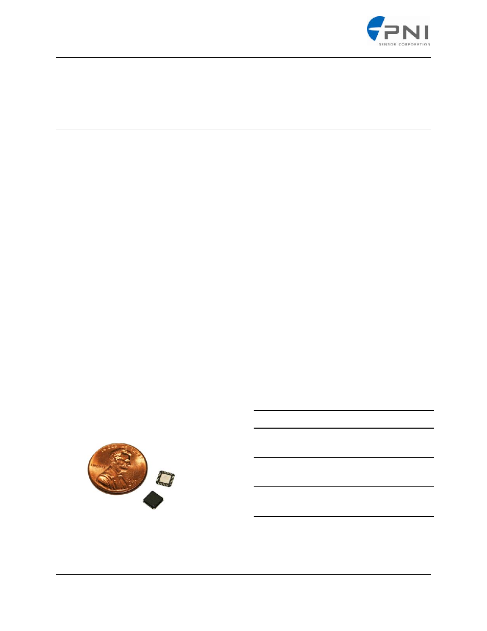
Ultra-low magnetic signature in Die form
Flexible supply voltage: 2.2 to 5.0 V
Fast sample rate: up to 2000 samples/second
Wide dynamic range: 96 dB (16 bits) in
hardware with 18 dB (3 bits) additional gain
scaling available
Fully digital interface: SPI protocol
Applications
Compassing
Magnetometer instruments
Magnetic object sensing
Magnetic ink sensing
Ordering Information
Name Part
#
MOQ
Pkg.
RoHS
Compliant
26 pad Die
10174
1,000
tray
Yes
28 pin MLF
12576
5000
reel
Yes
28 pin MLF
12576P
1
cut-
tape
Yes
Table 1
PNI Corporation 133 Aviation Blvd., Suite 101, Santa Rosa, CA 95403‐1084 USA Updated 27‐April‐09
Phone: (707) 566‐2260, Fax: (707) 566‐2261, Web: www.pnicorp.com
Document Outline
- General Description
- Features
- Applications
- Parameter
- Parameter voltage and current levels
- Vila
- Iilb
- Vol
- Iola
- 5 VDC
- 1
- 26
- VSTBY
- DP
- VDD
- Input protection clamp diode. Connect to VDD
- 2
- 27
- SCLK
- DI
- IBT
- Serial Clock input for SPI port. 1 MHz maximum (Rext = 100 kHz)
- 3
- 28
- MISO
- DO
- OB2
- Serial data output (Master In Slave Out)
- 4
- 1
- MOSI
- DI
- IBA
- Serial data output (Master Out Slave In)
- 5
- 3
- SSNOT
- DI
- IBA
- Active low chip select for SPI port
- ---
- 2
- Not Connected
- 6
- 4
- AVDD
- AP
- VDD
- Supply voltage for analog section
- 7
- 5
- AVSS
- AP
- VSS
- Ground pin for analog section
- 8
- 6
- +ZDRV
- DO
- OB3
- Z sensor drive output
- 9
- 7
- +ZIN
- AI
- AIB
- Z sensor sense input
- 10
- 8
- -ZIN
- AI
- AIB
- Z sensor sense input
- 11
- 9
- -ZDRV
- DO
- OB3
- Z sensor drive output
- 12
- 10
- +YDRV
- DO
- OB3
- Y sensor drive output
- 13
- 11
- +YIN
- AI
- AIB
- Y sensor input
- 14
- 12
- DVDD
- DP
- VDD
- Supply voltage for digital section
- 15
- 13
- -YIN
- AI
- AIB
- Y sensor input
- 16
- 14
- -YDRV
- DO
- OB3
- Y sensor drive output
- 17
- 15
- +XDRV
- DO
- OB3
- X sensor drive output
- 18
- 16
- +XIN
- AI
- AIB
- X sensor sense input
- 19
- 17
- -XIN
- AI
- AIB
- X sensor sense input
- 20
- 18
- -XDRV
- DO
- OB3
- X sensor drive output
- 21
- 19
- DVSS
- DP
- VSS
- Ground pin for digital section
- ---
- 20
- Not connected
- 22
- 21
- COMP
- DO
- OB1
- Comparator output. Used for diagnostics.
- 23
- 22
- RESET
- DI
- IBA
- Rest input
- 24
- 23
- DRDY
- DO
- OB1
- Data ready
- 25
- 24
- DHST
- DIO
- IOIA
- High speed oscillator output. Output is ½ clock speed. Use for diagnostics
- 26
- 25
- REXT
- AI
- AIB
- External timing resistor for high speed clock. 100 k ohm typical
- Exposed Paddle (center Pad)
- Connect to analog ground
- MOSI – Master Out Slave In
- SSNOT – Slave Select
- SCLK – Serial Clock
- MISO – Master In Slave Out
- RESET
- DRDY – Data Ready
- DHST – High Speed Oscillator Test
- PS0, PS1, and PS2 – Period Select
- ODIR – Oscillator Direction
- MOT – Magnetic Oscillator Test
- ASO & ASI – Axis Select
- Function
- AS1
- AS0
- 2 MHz scaling
- 0
- 0
- X axis
- 0
- 1
- Y axis
- 1
- 0
- Z axis
- 1
- 1
- Pad
- Function
- X (mm)
- Y (mm)
- 1
- VSTBY
- –655
- 968
- 2
- SCLK
- –755
- 968
- 3
- MISO
- –893
- 968
- 4
- MOSI
- –1012
- 968
- 5
- SSNOT
- –1128
- 968
- 6
- AVDD
- –1125
- 226
- 7
- AVSS
- –1125
- 62
- 8
- APZDRV
- –1125
- –81
- 9
- APZIN
- –1134
- –966
- 10
- ANZIN
- –1012
- –966
- 11
- ANZDRV
- –893
- –966
- 12
- APYDRV
- –448
- –966
- 13
- APYIN
- –3
- –966
- 14
- DVDD
- 115
- –966
- 15
- ANYIN
- 237
- –966
- 16
- ANYDRV
- 357
- –966
- 17
- APXDRV
- 802
- –966
- 18
- APXIN
- 1118
- –403
- 19
- ANXIN
- 1118
- –312
- 20
- ANXDRV
- 1118
- –189
- 21
- DVSS
- 1118
- 225
- 22
- COMP
- 1126
- 968
- 23
- RESET
- 1008
- 968
- 24
- DRDY
- 887
- 968
- 25
- DHST
- 768
- 968
- 26
- REXT
- 650
- 968
- Reflow Parameter
- Temperature (°C)
- Time (sec)
- Preheat Temperature (TSmin to TSmax)
- 150°C – 200°C
- 60-180
- Temperature TL (typical solder melting point)
- >218°C
- TSmax to TL Ramp-up Rate
- 3°C/second max
- Peak Temperature TP
- 260°C
- Time 25°C to Peak TP
- 6 minute max
- Time Maintained Above Temperature TL (tL)
- 218°C
- 60-120
- Soak (time within 5° of actual Peak TP)
- 10-20
- Ramp-down Rate
- 4°C/second max
- Parameter voltage and current levels
- Parameter