KEPCO KIT 219-0452, BIT 4886 Firmware Upgrade for BOP 100-1M-4886-25968 User Manual
Page 11
021704
228-1481 REV 3
11
KEPCO, INC. " 131-38 SANFORD AVENUE " FLUSHING, NY. 11352 U.S.A. " TEL (718) 461-7000 " FAX (718) 767-1102
http://www.kepcopower.com " email: [email protected]
DIAG:OUTP n
(n = hex character)
DIAG:OUTP?
(Returns hex charac-
ter)
DIAG:OUTP n controls the limit DAC values when the output is set to OFF. The values
can either be set to maximum or to a user determined limit value (using the
DIAG:OFFLimit commands. The SYST:SEC:IMM command sets DIAG:OUTP n = 0.
DIAG:OUTP 0 = the default. This sets both voltage and current limit channels to 0 when
the output is off. The four bits of the hex character are defined as follows:
Bit 0 = 1 sets voltage limit to maximum when in Voltage mode and the output is off.
Bit 1 = 1 sets current limit to maximum when in Current mode and the output is off.
Bit 2 = 1 sets voltage limit to value determined by the DIAG:OFFLimit:VOLT com-
mand when the output is off.
Bit 3 = 1 sets current limit to value determined by the DIAG:OFFLimit:CURR com-
mand when the output is off.
For example, DIAG:OUTP 3 = sets both voltage and current limit to maximum. This
can be useful for battery applications where the limit channel can allow the battery to
discharge the battery voltage. Using both the maximum and DIAG:OFFLimit options
(e.g., bits 0 and 2) at the same time is not recommended - the maximum value over-
rides the DIAG:OFFLimit setting.
DIAG:SAV
n/a
DIAG:SAV stores variables established by SYST:SET. (See PAR. 5.2.3 and B.82)
DIAG:WIN xx
(xx = hex value from 10
to 40)
1
DIAG:WIN?
(Returns window
value xx (hex)
Allows user to specify value in LSB’s for error window used for detection of output voltage
or output current measurement errors (default = 32). Error window value can only be
set between 16 (10 Hex) and 64 (40 Hex) using one two-digit hex character (xx)
1
.
Query returns 2-digit hex character xx.
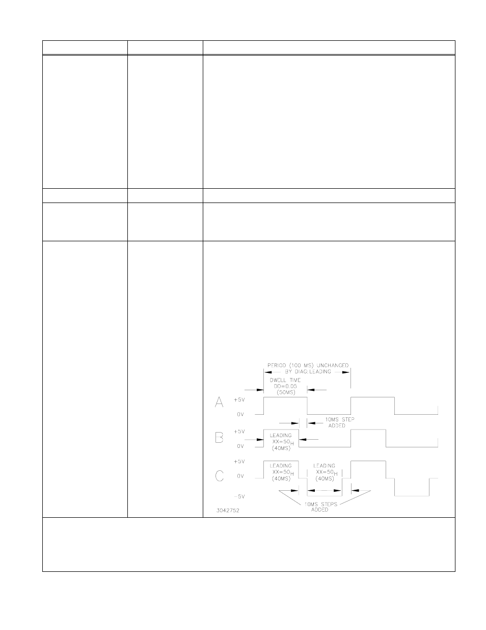
DIAG:LEADING xx
(xx is the time in half mil-
liseconds increments)
(hex)
DIAG:LEADING?
returns xx (hex), the
time in half millisec-
onds increments)
xx establishes max dwell time for a two-step list. If the dwell time DD for the two-step list
exceeds xx, a step is inserted with voltage = 0V for (DD - xx). MSTS default = 50.
Consider the following:
LIST:VOLT 0,5
Two step list, 0V then 5V.
LIST:DWEL .05
Dwell time of 50 ms
LIST:COUNT 0
Repeat continuously.
OUTP ON
Output enabled.
VOLT:MODE LIST Run program
The above list would normally produce a continuous square wave, 50ms at 0V, 50ms
at 5V (Fig A). If DIAG:LEADING 50 (40 ms) is issued, the square wave changes to
60ms at 0V, 40ms at 5V as follows: the first 1/2 cycle = 50ms at 0V, the second 1/2
cycle = 40ms (the limit set by DIAG:LEADING) at 5V, then 10ms (50 - 40 = 10) at 0V
(Fig B). If LIST:VOLT 0,5 is changed to LIST:VOLT -5,5 both 1/2 cycles will show
10ms steps at 0V (Fig C).
1 The default window value of 32 indicates a 32 LSB margin for error during readback. The value for Readback is arrived at by taking 16 samples
of voltage or current and averaging them. A readback error is produced when the calculated readback value (with calibration constants applied)
exceeds the maximum readback (calculated readback + error window) or minimum readback (calculated readback – error window). Increasing
the error window can avoid undesired errors. For example, in cases where the LIST command is used to produce a square wave output, over-
shoot inherent in the characteristics of the power supply can sometimes cause the readback average to increase enough to cause a readback
error. Increasing the error window allows the square wave to be generated without producing an error.
TABLE 5-1. ENHANCED OPERATION - ERROR RESPONSE (CONTINUED)
COMMAND
QUERY
DESCRIPTION