Figure 10 – add-in card tx connection diagram – Teledyne LeCroy QPHY-PCIe3-Tx-Rx User Manual
Page 21
QPHY-PCIE3-TxRx
Operator’s Manual
923662 Rev B
17
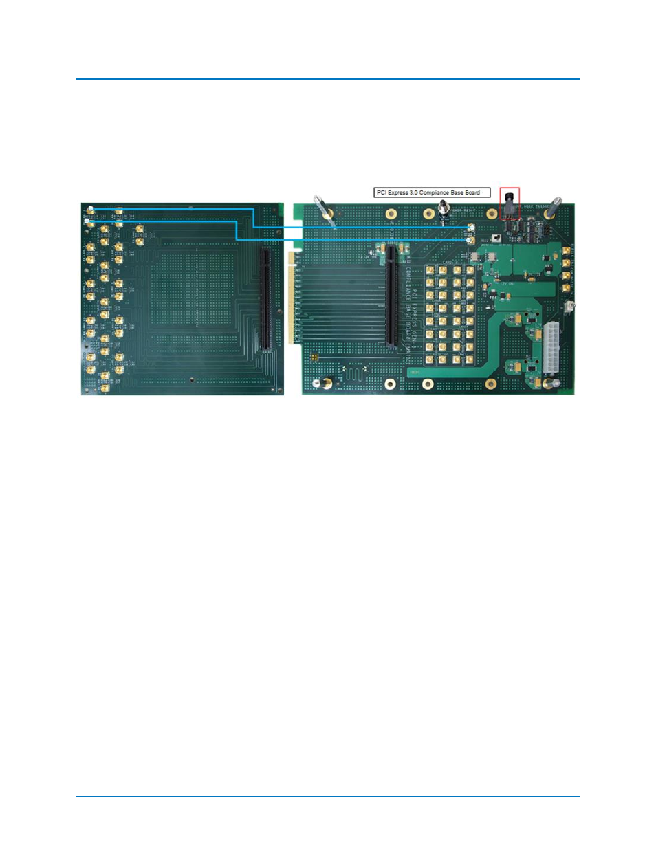
A toggle switch on the CLB controls the clock to Rx lane0. Every time the switch is pressed,
J5/J85 sends clock toggle to Rx lane0, which will cause the compliance pattern to cycle to the
next pattern.
The diagram below shows the location of the toggle switch (circled in red). The blue lines
indicate the required SMP to SMP cable connections to allow the signal caused by pressing the
toggle button to be coupled into the RX lane 0 that goes to the add in card.
Figure 10
– Add-In Card Tx connection diagram.
Below are the built-in compliance patterns for all PCIE Gen3 Add-in Cards and Systems,
starting from the first pattern after power up (2.5Gbps Gen 1 compliance pattern). The cycle
repeats after pattern 14. Press the toggle sufficient times to go from the current pattern to the
desired pattern.
1. 2.5Gbps Gen1 compliance pattern
2. 5.0Gbps Gen2 compliance pattern with 3.5dB de-emphasis
3. 5.0Gbps Gen2 compliance pattern with 6dB de-emphasis
4. 8.0Gbps Gen3 compliance pattern with preset 0
5. 8.0Gbps Gen3 compliance pattern with preset 1
6. 8.0Gbps Gen3 compliance pattern with preset 2
7. 8.0Gbps Gen3 compliance pattern with preset 3
8. 8.0Gbps Gen3 compliance pattern with preset 4
9. 8.0Gbps Gen3 compliance pattern with preset 5
10. 8.0Gbps Gen3 compliance pattern with preset 6
11. 8.0Gbps Gen3 compliance pattern with preset 7
12. 8.0Gbps Gen3 compliance pattern with preset 8
13. 8.0Gbps Gen3 compliance pattern with preset 9
14. 8.0Gbps Gen3 compliance pattern with preset 10