Solidtron, N-type semiconductor discharge switch, thinpak – Silicon Power CCS TA 14N40_N-Type Semiconductor Discharge Switch, ThinPak User Manual
Page 2
Performance Characteristics
T
J
=25
o
C unless otherwise specified
Measurements
Parameters
Symbol
Test Conditions
Min.
Typ.
Max.
Units
Anode to Cathode Breakdown Voltage
V
DR
V
GK
=0, I
A
=1mA
4
kV
Anode-Cathode Off-State Current
I
D
V
GK
=0V, V
AK
=4000V
T
J
=25
o
C
<50
100
uA
T
J
=125
o
C
100
800
uA
Turn-On Threshold Current
V
GK(TH)
V
AK
=V
GK
, I
AK
=1mA , see Note 1
5
mA
Gate-Cathode Leakage Current
I
GK(lkg)
V
GK
=0V, see Note 1
20
uA
Anode-Cathode On-State Voltage
V
T
I
T
=400A
T
J
=25
o
C
1.7
V
Ig = 500 mA
T
J
=125
o
C
1.9
V
Turn-on Delay Time
t
D(ON)
0.75 uF Capacitor discharge
200
ns
Pk Rate of Change of Current (measured)
dI/dt
V
AK
= 3.95 kV
T
J
=25
o
C
30
kA/us
Peak Anode Current
I
P
R
gk
= 10 ohms, Ls = 90 nH
10
kA
Gate di/dt =100 A/us
Notes:
1. Measurements made with a 10 Ohm shorting resistor connected between the gate and cathode.
2. Case Exterior Assummed to be 0.002" of 63sn/37pb solder applied directly to cathode bond area of thinPak.
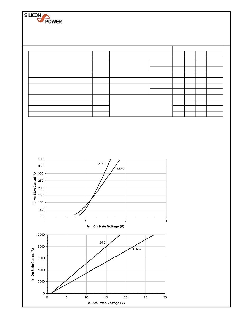
Typical Performance Curves
(unless otherwise specified)
Solidtron
TM
N-Type Semiconductor Discharge Switch,
ThinPak
TM
Data Sheet (Rev 0 - 05/12/08)
CCSTA14N40A10
275 Great Valley Parkway
Malvern, PA 19355
Ph: 610-407-4700
Fax: 610-407-3688
Figure 1.
Measured Low current
On-State Characteristics.
Figure 2.
Predicted high current
On-State Characteristics.
CAO 05/28/09
CAO 05/28/09